SSZT385 october 2019 TPS62088
When it comes to cost-effectively powering space-constrained, high-power-density applications, such as solid-state drive (SSD) or wearable equipment, wafer chip-scale package (WCSP) DC/DC converter solutions are widely used in the industry. The trend toward even tighter integration into system-in-package (SIP) modules poses an increasing challenge to established packaging techniques, forcing engineers to look for new ways of optimizing thermal performance in space-constrained applications.
Thermal performance and solution size, particularly maximum profile height, are very real challenges that every SIP designer experiences. As the designer of a low-form-factor SIP module for your next application, you may be searching for a power device that will fit in the tiny space you have and that will also stay cool while delivering the power you need for your system.
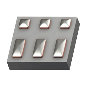
TI’s power chip-scale packaging (power WCSP) is a low-profile WCSP enhancement that focuses on thermal performance and current density optimization. Unlike a standard WCSP, which uses a fixed ball diameter (Figure 1a), power WCSP takes advantage of the flexibility of copper post sizes to increase the area of key interconnects like power pins, without having to increase the die size or infringe upon the spacing tolerance of surface-mount manufacturing technologies. The copper posts can be square or rectangular, with a total stack thickness as small as 85 µm (Figure 1b). The shape of the posts makes it possible to achieve a significant surface gain for critical pins, thereby increasing current-handling capacity as well as improving the heat transfer and thermal performance of the package. At the same time, the package height can be as low as 0.3 mm, enabling easy implementation into high-power-density and space-critical integrated solutions.

 Figure 1 6-pin standard WCSP package
(a); 6-pin power WCSP package (b)
Figure 1 6-pin standard WCSP package
(a); 6-pin power WCSP package (b)TI’s TPS62088 DC/DC converter demonstrates the thermal performance of power WCSP packaging. The TPS62088 is a 1.2-mm-by-0.8-mm, high-efficiency 2.4-V to 5.5-V input, 3-A DC/DC buck converter operating at a 4-MHz switching frequency. The device is available in two package options: either the standard WCSP (TPS62088YFP) or the new power WCSP (TPS62088YWC). Looking at the thermal properties of these otherwise identical devices in each package option allows us to make a clear comparison of the thermal performance of the two packaging technologies.
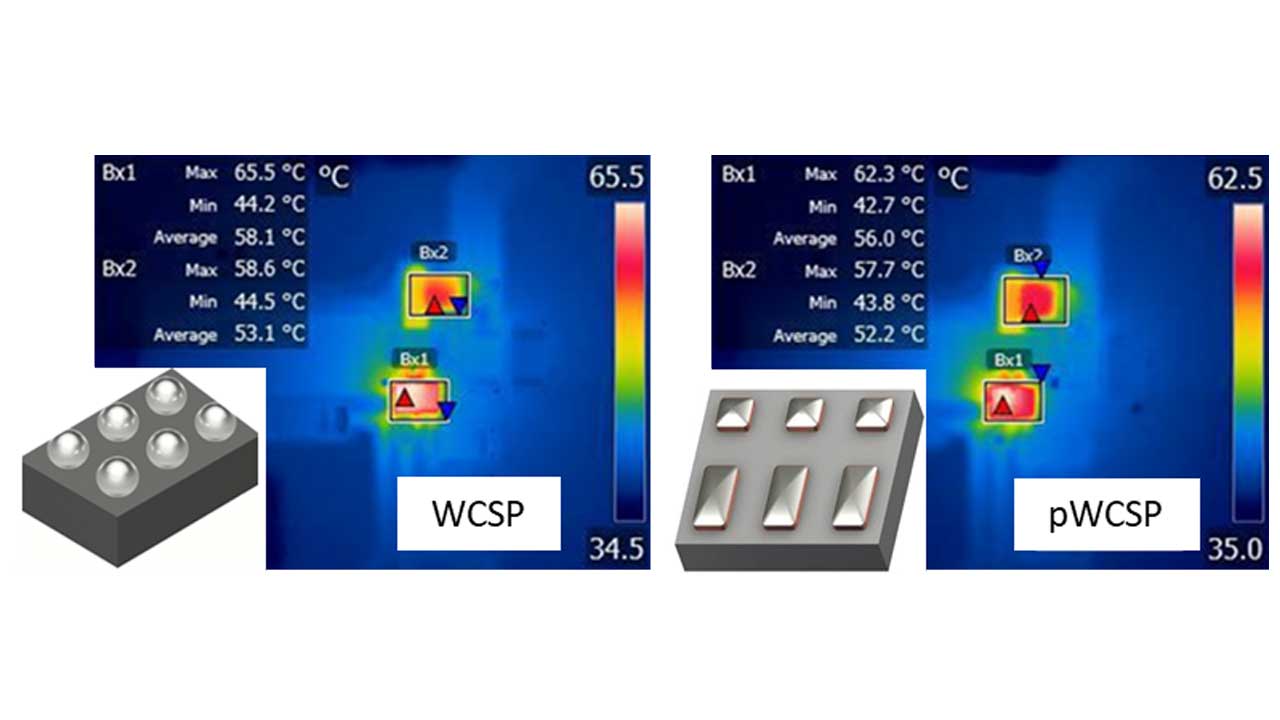
Figure 2a shows the thermal performance of the TPS62088YFP (WCSP) and Figure 2b shows the TPS62088YWC (power WCSP) operating at VIN = 5 V, VOUT = 1.8 V and IOUT = 3 A, taken at room temperature with an infrared camera. Due to very low junction-to-top characterization parameter values – ΨJT = 0.5-0.7°C/W for both packages – you can assume that the junction temperature is roughly equal to the case temperature. The results indicate that the temperature of the power WCSP device is reduced by as much as 3°C compared to the standard WCSP device, considering the device and printed circuit board (PCB) layout solution together.
The TPS62088YWC power WCSP version, while increasing power density by reducing profile height from 0.5 mm to 0.3 mm, enables you to optimize the thermal performance of your system by improving the heat transfer to the PCB through the larger bump structures. Of course, designing your application for optimal thermal performance implies paying attention to further aspects of the system as well. Proper PCB layout results in smaller junction-to-ambient and junction-to-board thermal resistance, thereby reducing the device junction temperature for a given dissipated power and board temperature. Wide power traces can also efficiently sink dissipated heat. Keep in mind that many system-dependent properties such as thermal coupling, airflow, added heat sinks and convection surfaces, and the presence of other heat-generating components, affect the power dissipation capabilities of a given device.
 Figure 2 Thermal performance of the
TPS62088 (measurement point: Bx1) operating at VIN = 5 V,
VOUT = 1.8 V and IOUT = 3 A taken at room temperature:
TPS62088YFP WCSP version (a); TPS62088YWC power WCSP version (b)
Figure 2 Thermal performance of the
TPS62088 (measurement point: Bx1) operating at VIN = 5 V,
VOUT = 1.8 V and IOUT = 3 A taken at room temperature:
TPS62088YFP WCSP version (a); TPS62088YWC power WCSP version (b)Many space-constrained applications like SIP modules, SSDs or wearable devices, require the total power solution, (not just the power IC), to fit in the thinnest spaces possible. The TPS62088YWC’s high switching frequency allows you to use tiny, low-form-factor 0.24-µH inductors to shrink the solution size to 15 mm2, and take full advantage of the 0.3-mm profile height for the whole power circuit.
Additional resources
- Read the application note, “AN-1112 DSBGA Wafer Level Chip Scale Package,” to learn more about surface-mount assembly techniques for this package type.
- See the Thermal Characteristics of Linear and Logic Packages Using JEDEC PCB Designs and IC Package Thermal Metrics application notes, for more details on how to use the thermal parameters.