SSZT554 January 2019 ADS1261
- 1
-
2
- 3
- 1. What Types of Noise Can You Expect to Find in ADCs?
- 2. How Is ADC Noise Measured and Specified?
- 3. What Is the Best Noise Parameter to Use for System Noise Analysis?
- 4. What Is ENBW and Why Is It Important?
- 5. How do you calculate the noise bandwidth of your system?
- 6. If You Add an External Amplifier to the Input of an ADC, How Does This Affect System Noise Performance?
- 7. Is There Such a Thing as Too Much Gain?
- 8. How Do You Calculate the Amount of Reference Noise Passing into Your System?
- 9. How Can You Reduce the Amount of Reference Noise Passing into Your System?
- 10. Can Clocks Affect Your ADC's Noise Performance?
One of the fundamental challenges in any high-resolution signal-chain design is ensuring that the system noise floor is low enough for the analog-to-digital converter (ADC) to resolve your signals of interest. For example, if you chose the TI ADS1261 – a 24-bit low-noise delta-sigma ADC – you could resolve input signals as low as 6 nVRMS at 2.5 SPS and a gain of 128 V/V.
From a system perspective, however, it’s not just the ADC’s noise that you need to worry about: all components, including amplifiers, voltage references, clocks and power supplies, contribute some noise. What’s the cumulative effect of these devices on your system’s noise? And more importantly, will your system be able to resolve your signals of interest?
To help you better understand system noise and apply this knowledge to your designs, I recently wrote a technical article series called “Resolving the Signal.” The series examines common noise sources in a typical signal chain and complements this understanding with methods to mitigate noise and maintain high-precision measurements.
Here are the 10 most critical questions and answers from the series to get you started designing with precision ADCs,
1. What Types of Noise Can You Expect to Find in ADCs?
 and Thermal Noise (Right)") Figure 1 Quantization Noise (Left) and Thermal Noise (Right)
Figure 1 Quantization Noise (Left) and Thermal Noise (Right)Do thermal and quantization noise affect low- and high-resolution ADCs equally? Read part 1, “Introduction to Noise in Delta-Sigma ADCs,” to find out.
2. How Is ADC Noise Measured and Specified?
 and Input-short Test Setup (Right)") Figure 2 Sine-wave-input Test Setup (Left) and Input-short Test Setup (Right)
Figure 2 Sine-wave-input Test Setup (Left) and Input-short Test Setup (Right)Which ADCs use which type of measurement method? Read more about noise measurement methods and specifications in part 2.
3. What Is the Best Noise Parameter to Use for System Noise Analysis?
Part 3 takes these claims one step further with a design example that uses both noise-free resolution and input-referred noise to define a system noise parameter. Which one enables the quickest, most adaptable solution? Read the article to discover the answer.
4. What Is ENBW and Why Is It Important?
; Narrow ENBW Leads to Less Noise (Right)") Figure 3 Wide ENBW Leads to More Noise
(Left); Narrow ENBW Leads to Less Noise (Right)
Figure 3 Wide ENBW Leads to More Noise
(Left); Narrow ENBW Leads to Less Noise (Right)What system components contribute to ENBW? Read part 4 to learn more.
5. How do you calculate the noise bandwidth of your system?
If your signal chain has multiple filter components, you must calculate the ENBW for each component by combining all downstream filters in the signal chain. To combine filters, plot them as magnitude (in decibels) vs. frequency and add them point by point.
For example, to calculate the noise contribution of the amplifier in Figure 4, you would have to combine the amplifier’s bandwidth with the anti-aliasing filter, the ADC’s digital filter and any post-processing filters. You could ignore the electromagnetic interference (EMI) filter in this case since it is upstream relative to the amplifier.
 Figure 4 Typical Signal Chain Showing
Multiple Sources of Filtering
Figure 4 Typical Signal Chain Showing
Multiple Sources of FilteringSince this can be complicated, read part 5 to learn ENBW approximation methods to simplify your analysis.
6. If You Add an External Amplifier to the Input of an ADC, How Does This Affect System Noise Performance?
 Figure 5 “Noiseless” ADC and Amplifier
Preceded by Total Noise, Referred-to-input
Figure 5 “Noiseless” ADC and Amplifier
Preceded by Total Noise, Referred-to-inputUnfortunately, the measured output noise must refer back to the input, since input-referred noise is the specification used in most ADC data sheets. Assuming that the amplifier and ADC noise are uncorrelated, take the root-sum-square (RSS) of both values to determine the total output-referred noise. You also need to scale the amplifier noise by the amplifier’s gain, GAMP. Equation 1 shows the resulting output-referred noise:
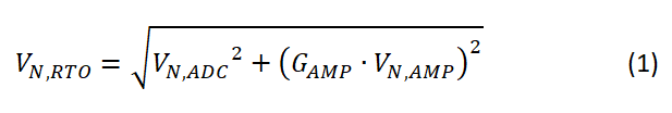
How do you translate this to input-referred noise? And what are the ramifications of the gain scaling factor, GAMP? Read part 6 to find out.
7. Is There Such a Thing as Too Much Gain?
 Figure 6 Comparing Noise Performance of Different Amplifiers plus the ADS1261 as a Function of Gain
What are the key takeaways from this example and the plot in Figure 6? Read part 7, “The Effects of Amplifier Noise on Delta-Sigma ADCs,” to learn more.
8. How Do You Calculate the Amount of Reference Noise Passing into Your System?
 Figure 7 Reference Noise, ADC Noise and Total Noise as a Function of FSR Utilization
What do the key points – A, B and C – on this plot represent? And how does changing your input signal vs. changing your system gain affect reference noise? Find the answers to these questions in part 8.
9. How Can You Reduce the Amount of Reference Noise Passing into Your System?
, 24 Hz (Middle), 96 Hz (Right)") Figure 8 Limiting ENBW Reduces Total
Noise: 0.6 Hz (Left), 24 Hz (Middle), 96 Hz (Right)
Figure 8 Limiting ENBW Reduces Total
Noise: 0.6 Hz (Left), 24 Hz (Middle), 96 Hz (Right)Read part 9 to learn about how your reference configuration can also reduce the amount of reference noise passing into your system.
10. Can Clocks Affect Your ADC's Noise Performance?
 Figure 9 Clock Signal Showing Sampling-edge Variation Caused by Jitter
To learn how clocks cause additional errors, as well as ways to reduce system noise due to clocking, read part 10.
While these are some of the most important questions answered in the “Resolving the Signal” series, I covered many more topics and examples to help you get the best noise performance out of your high-resolution, delta-sigma ADC signal chain. Read the series to learn more, and if you have any additional questions, feel free to post them in the comments below.