SSZTAB5 march 2017 UCC27524A
I hope you’ve had a chance to watch our video series, “Know Your Gate Driver.” Although often overlooked, gate drivers are responsible for a lot of the heavy lifting in systems like power supplies and motor-control systems. I like to think of a gate driver as a muscle! The video series explains how while highlighting key gate-driver parameters. Topics range from negative-voltage handling and delay matching to wide VDD and operating temperature ranges. In this blog post, I’ll explain these topics a bit more fully.
Negative Voltage
Negative-voltage handling in a gate driver is the ability to withstand negative voltages at the input and output. These unwanted voltages can result from parasitic inductances caused by switching transitions, leakage or even poor layout. A gate driver’s ability to survive negative voltages is critical for a robust, reliable solution.
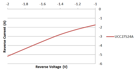
Figure 1 shows how TI gate drivers survive negative voltages resulting from large amounts of undershoot and overshoot, with no damage to the integrated circuit.
 Figure 1 Negative Reverse Voltage
Handling
Figure 1 Negative Reverse Voltage
HandlingDelay Matching
Delay matching is a specification that shows how accurately the internal propagation delays between channels are matched. If a signal is simultaneously applied at the inputs of two channels, the time delay at the outputs of both channels is the delay-matching figure. The smaller the delay-matching specification, the better performance the gate driver can achieve.
Delay matching has two main benefits:
- It ensures the driving of paralleled MOSFETs simultaneously with a minimal turn-on delay difference.
- It eases the paralleling of gate-driver outputs to effectively double current capability and eases the driving of parallel power switches.
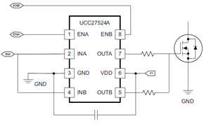
TI’s UCC27524A has extremely accurate 1ns (typical) delay matching, which can increase the drive current from 5A to 10A. Figure 2 shows the UCC27524A’s A and B channels combined into one driver. The INA and INB inputs are connected together, as are OUTA and OUTB. One signal controls the paralleled combination.
 Figure 2 The UCC27524A with Paralleled
Outputs to Double Drive-current Capability
Figure 2 The UCC27524A with Paralleled
Outputs to Double Drive-current CapabilityOne result of accurate delay matching is an increase in power density. The need for higher power densities is a trend in applications like power factor correction (PFC) and synchronous rectification blocks of isolated power supplies, DC/DC bricks and solar inverters, where designers are restricted to the same size (or smaller!) for the same amount of output power.
Wide VDD Range
When I refer to having a “wide VDD range,” I am referring to the positive supply voltage connected to the drain of the MOSFET or to the collector of the insulated gate bipolar transistor (IGBT). For gate drivers, the VDD defines the range of drive output.
There are three benefits of having a wide VDD range:
- It provides the flexibility in your system design to use the same driver with different operating voltages and different types of power switches.
- It offers robustness in noisy environments or when using low-quality power supplies, effectively preventing your system from being damaged by overshoot or undershoot.
- Drivers with a wide VDD range can be used in split-rail systems, such as driving IGBTs with both positive and negative supplies.
Overall, a wide VDD range gives you flexibility in your system design and robustness in extreme conditions.
Operating Temperature Range
An often-overlooked detail is under what conditions the gate driver was tested. You will typically see gate drivers tested at room temperature, which is usually 25°C. The minimum and maximum are characterized over the entire operating temperature range and added statistical guardband.
Do not ignore the operating temperature range, because the minimum and maximum specifications can vary significantly when they are guaranteed over -40°C to 125°C versus only at room temperature. Most TI gate-driver devices are specified from -40°C to 125°C or at 140°C. This provides you with consistent performance and robustness under extreme temperatures. Taking this detail from data sheets into account makes it easier for you to choose the correct gate driver.
As you can see, there are many parameters to consider when choosing your system’s gate driver. Be sure to watch our video series and ask any questions in our E2E community.

Additional Resources
- Check out the featured products for MOSFET and IGBT gate drivers.
- Read these Power House blog posts:
- “Don’t forget the gate driver: it’s the muscle.”
- “How to achieve higher system efficiency – part one: high-current gate drivers.”
- “How to achieve higher system efficiency – part two: high-speed gate drivers.”