SSZTAE5 february 2017 LM5175
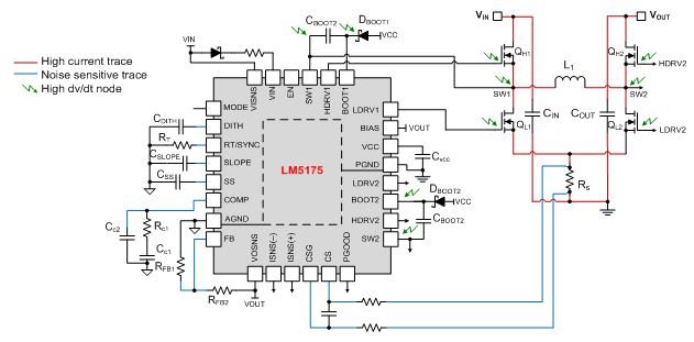
Layout is very critical to the successful operation of a buck-boost converter. A good layout begins by identifying these critical components, as shown in Figure 1:
- High di/dt loops or hot loops.
- High dv/dt nodes.
- Sensitive traces.
 Figure 1 Identifying High Di/dt Loops,
High Dv/dt Nodes and Sensitive Traces
Figure 1 Identifying High Di/dt Loops,
High Dv/dt Nodes and Sensitive TracesFigure 1 shows the high di/dt paths in the LM5175 four-switch buck-boost converter. The most dominant high di/dt loops are the input-switching current loop and output-switching current loop. The input loop consists of an input capacitor (CIN), MOSFETs (QH1 and QL1), and a sense resistor (Rs). The output loop consists of an output capacitor (COUT), MOSFETs (QH2 and QL2), and a sense resistor (Rs).
The high dv/dt nodes are those with fast voltage transition. These nodes are switch nodes (SW1 and SW2), boot nodes (BOOT1 and BOOT2), and gate-drive traces (HDRV1, LDRV1, HDRV2 and LDRV2), along with their return paths.
The current-sense traces from resistor Rs to the integrated circuit (IC) pins (CS and CSG), the input and output sense traces (VISNS, VOSNS, FB), and the controller components (SLOPE, Rc1, Cc1, Cc2) form the noise-sensitive traces. They are shown in blue in Figure 1.
For good layout performance, minimize the loop areas of high di/dt paths, minimize the surface areas of high dv/dt nodes, and keep the noise-sensitive traces from the noisy (high di/dt and high dv/dt) portions of the circuit. In the other two installments of this series, I’ll look at each of these in detail in the context of the four-switch buck-boost converter. My next topic will include an example for optimizing hot loops.
Additional Resources
- Check out my 2016-2017 Power Supply Design Seminar topic, “Under the hood of a non-inverting buck-boost converter.”