SSZTCM4 june 2015 DS80PCI810
In a high-speed printed circuit board (PCB), a via is notorious for degrading signal-integrity performance. However, using via structures is unavoidable. In a typical board, components are placed on the top, while differential pairs are routed in inner layers where they lower electromagnetic radiation and pair-to-pair crosstalk. Vias must be used to connect components on the board’s surface to the inner layers.
Fortunately, it’s possible to design a transparent via that minimizes performance impact. In this post, I’ll discuss the following:
- Basic elements of vias
- Electrical properties of vias
- A method to build a transparent via
- Test results of a differential via structure
Basics of a via Structure
Let’s start by examining the elements of a simple via that connects a top trace to an inner trace. Figure 1 is a 3-D diagram showing a via construction. There are four basic elements: the signal via, via stub, via pad and anti-pad.
Vias are metal cylinders that plate through holes between the top and bottom layers of a board. Signal vias connect traces at different layers. Via stubs are the unused part of the via. Via pads are donut-shaped pads that connect the vias to the top or the inner traces. Anti-pads are the circular clearances in each power or ground layer that prevent electrical short to the plane.
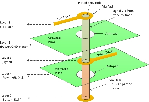 Figure 1 3-D Diagram of a Single
via
Figure 1 3-D Diagram of a Single
viaElectrical Properties of via Elements
Let’s walk down the signal path to visualize the electrical property of each via element, shown in Figure 2.
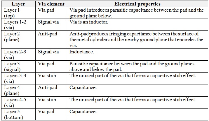 Figure 2 Electrical Properties of the
via Elements Shown in 3-D Diagram of a Single via
Figure 2 Electrical Properties of the
via Elements Shown in 3-D Diagram of a Single viaA simple via is a series of π-networks made of capacitance-inductance-capacitance (C-L-C) elements formed within two adjacent layers. Figure 3 shows the effect of the via dimensions.
 Figure 3 Intuitive Effect of via
Dimensions
Figure 3 Intuitive Effect of via
DimensionsBy balancing the amount of inductance and parasitic capacitance, it’s possible to construct a via with the same characteristic impedance as the trace, thus becoming transparent. There’s no simple equation that translates via dimensions into the C and L elements. A 3-D electromagnetic (EM) field solver can predict the impedance of a structure based on the dimensions used in a PCB layout. By repeatedly adjusting the structure’s dimensions and running 3-D simulations, it’s possible to optimize the via dimension to achieve the desired impedance and bandwidth requirements.
Building a Transparent Differential via
As discussed in my previous post, a differential pair must be implemented with a high degree of symmetry between the A and B wires. The pairs are routed in the same layers, and if there’s a need for a via, it must be implemented in both wires at locations close by. Because the two vias of the differential pair are in close proximity, instead of using two separate anti-pads, an oval anti-pad shared by the two vias reduces parasitic capacitance. A ground via is also placed next to each via so that they provide ground-return paths for the A and B vias.
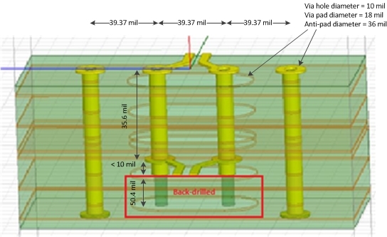 Figure 4 A GSSG Differential via with
Back-drill
Figure 4 A GSSG Differential via with
Back-drillFigure 4 shows a ground-signal-signal-ground (GSSG) differential via structure example. The distance between the two adjacent vias is called a via pitch. A smaller via pitch introduces more mutual coupling capacitance.
Don’t forget that the via stub produces severe degradation to high-speed signal integrity at above 10Gbps. Fortunately, there’s a back-drill PCB manufacturing process that precisely drills through the unused via cylinder. Determined by the manufacturing process tolerance, back-drilling removes the unused via metal and minimizes the via stub to less than 10mils.
A 3-D EM simulator is used to design a differential via with the desired impedance and bandwidth. This is an iterative process that repeatedly adjusts the via dimensions and runs EM simulations until achieving the desired impedance and bandwidth.
How to Verify Performance
The differential via design shown in Figure 4 was built and tested. The test sample consists of a pair of differential traces at the top layer, followed by a differential via to the inner traces, then a second differential via connects to the BGA landing pads at the top layer again. The total length of the signal path is about 1,330mils. I measured its differential impedance with a differential time-domain reflectometer (TDR), its bandwidth by using a network analyzer, and its effect on the signal by measuring the data-eye opening with a high-speed oscilloscope. Figure 5, Figure 6, and Figure 7 show the impedance, bandwidth, and eye diagrams, respectively. The left-side plots are the test results with back-drilling, while the right-side plots are those without back-drilling. From the bandwidth plot in Figure 7, it’s clear that back-drilling is necessary to achieve high performance at data greater than 10Gbps.
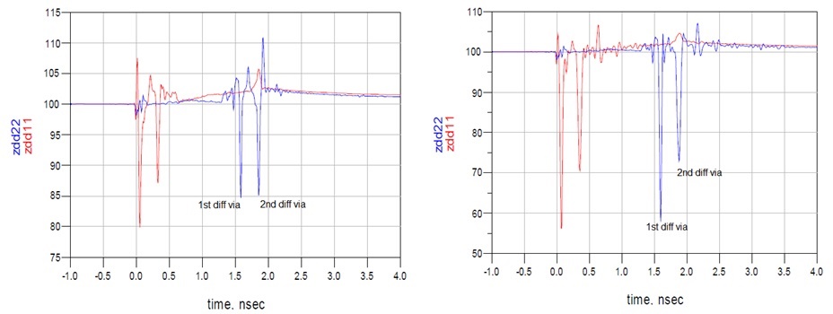
With back-drill (left), ZDIFF is about 85Ω. Without back-drill (right), ZDIFF is about 58Ω.
Figure 5 TDR Impedance Plots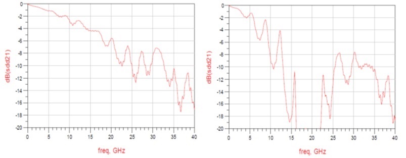
Insertion loss (left) at 12.5GHz is about 3dB. Insertion loss (right) at 12.5GHz is more than 8dB.
Figure 6 Frequency Responses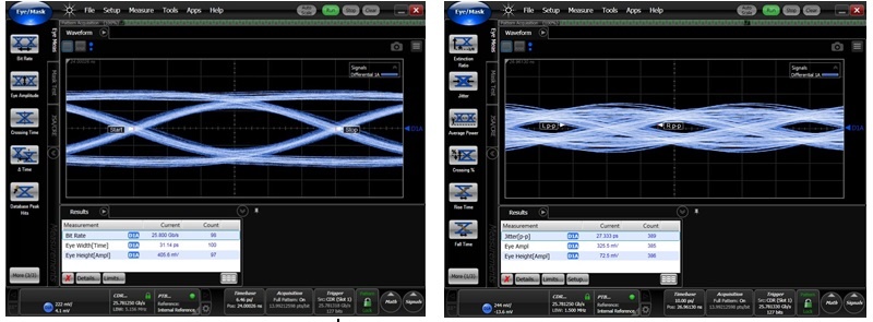
With back-drill (left), data eye is open. Without back-drill- (right), data eye is closed.
Figure 7 Data-eye Diagrams at 25GbpsTI has a rich portfolio of high-speed signal-conditioning integrated circuits (ICs) such as retimers and redrivers. They help mitigate imperfections and high insertion loss from all types of differential pairs, enabling reliable data communication and extending transmission distance for modern systems.
Leave a note below – I’d love to hear your feedback on this post or anything you’d like to learn in future “differential pairs” posts.
Additional Resources
- See an overview of TI’s portfolio of low-voltage differential signaling (LVDS), multipoint LVDS (MLVDS), signal-conditioning retimers and redrivers.
- Find out about TI’s two-port 40 Gigabit Ethernet (40GbE)/10GbE quad small form-factor pluggable (QSFP+) signal conditioner reference design.
- Learn about TI’s Peripheral Component Interconnect Express (PCIe) Gen-3 cards with this DS80PCI810 linear redriver reference design.
- Read more about the WEBENCH® Interface Designer tool, which helps designers use TI signal-conditioning ICs to solve differential pairs’ impairments.