SSZTCN2 june 2015 TPS544B20 , TPS544C20
Enterprise servers and switches, storage attach networks and base stations are increasingly using power supplies with PMBus to easily configure, control and monitor critical voltage rails such as high-current ASICs, DSPs, FPGAs and DDR memory core without software programming.
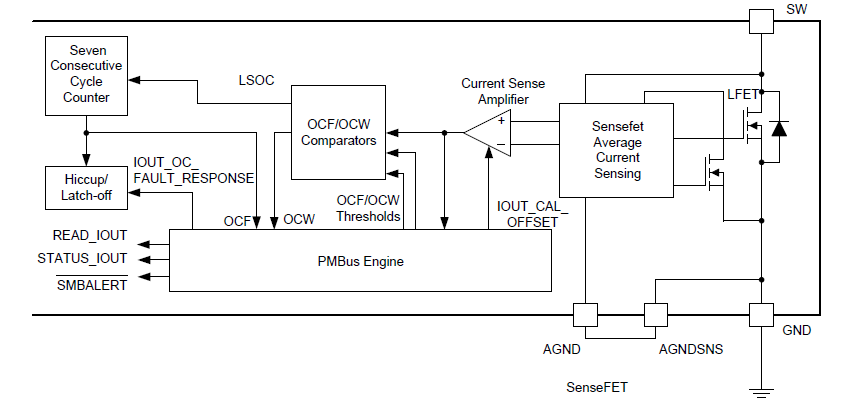
Monitoring output voltage, current and temperature is useful for board characterization and real-time, remote monitoring of high-power data centers. DC/DC converters such as TI’s 20A TPS544B20 and 30A TPS544C20 provide this capability. These devices are able to sense the average output current using an internal MOSFET sensor. The sensor carries a scaled-down version of the current through the main power MOSFET to enable current monitoring and better overcurrent threshold accuracy compared to inductor DCR current sensing. As well, there is minimal temperature variation and dependence on the inductor power loss thus enabling the end user to select a lower DCR inductor to improve efficiency even further, while reducing cost and size.
 Figure 1 TPS544B20 and TPS544C20 MOSFET
Current Sensing
Figure 1 TPS544B20 and TPS544C20 MOSFET
Current SensingWhen the power supply is assembled on the board, there can be layout-related systemic errors that introduce additional variation in the output current sense and measurement accuracy. Fortunately, the TPS544B20 and TPS544C20 include a PMBus command “IOUT_CAL_OFFSET” that can be used to improve current sensing and measurement accuracy post assembly.
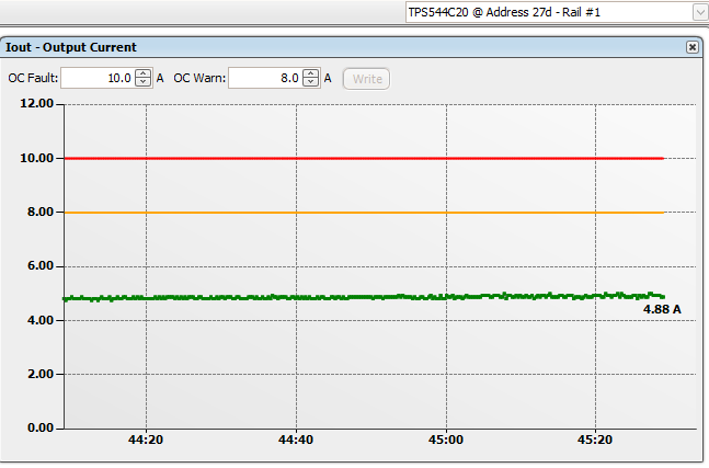
 Figure 2 TPS544B20 and TPS544C20 Output
Current Monitoring via TI Fusion Digital Power™ Gui
Figure 2 TPS544B20 and TPS544C20 Output
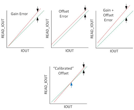
Current Monitoring via TI Fusion Digital Power™ GuiThe current sense error has two components: Gain and Offset. Gain is a multiplicative factor (i.e. IOUTx0.98 = gain is 2% low). Offset is an additive factor (i.e.READ_IOUT=IOUT+1A). As the name implies, IOUT_CAL_OFFSET adjusts the offset. In reality, the device has both gain and offset error. Using the IOUT_CAL_OFFSET command allows the end user to “center” the output current reading at a certain point, which mitigates the cumulative effect of a gain error. The best place to calibrate is in the center of the design’s operating range. The IOUT_CAL_OFFSET command is used to compensate for offset errors in the READ_IOUT
results and the IOUT_OC_FAULT_LIMIT and IOUT_OC_WARN_LIMIT thresholds. The default setting is 0A (amperes). The resolution of this command is 62.5mA (milliamperes) and the range is +3937.5mA to -4000mA. The contents of this register can be stored to the TPS544B20 or TPS544C20 non-volatile memory using The STORE_USER_ALL command.
 Figure 3 TPS544B20 and TPS544C20
IOUT_CAL_OFFSET PMBus Command in TI Fusion Digital Power GUI
Figure 3 TPS544B20 and TPS544C20
IOUT_CAL_OFFSET PMBus Command in TI Fusion Digital Power GUITo “calibrate” the current measurement in ICT using the IOUT_CAL_OFFSET command, force a known load current to the output of the TPS544B20 or TPS544C20 and use IOUT_CAL_OFFSET to adjust READ_IOUT until it matches the known load value. For example, the end user might force a 20A load current with a resistor or DC load, read READ_OUT through the Fusion Digital Power GUI and get 22A. They could then apply IOUT_CAL_OFFSET = -2A to set the READ_IOUT to the actual Iout of 20A.
 Figure 4 READ_IOUT Gain and Offset
Errors before and after Calibrating the READ_IOUT Offset
Figure 4 READ_IOUT Gain and Offset
Errors before and after Calibrating the READ_IOUT OffsetWith this PMBus command, the user can tighten the output current measurement accuracy through the TPS544B20 or TPS544C20 PMBus interface eliminating any post-assembly errors.
Download the TI Design, High density 30W DC/DC buck converter with the inductor mounted over the converter to save space to get started on your design.