SWRA636C November 2019 – December 2020 CC1352P , CC2652P
A.2 Layout
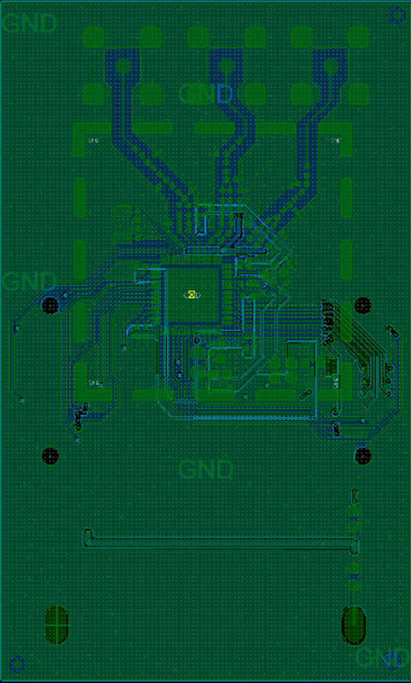
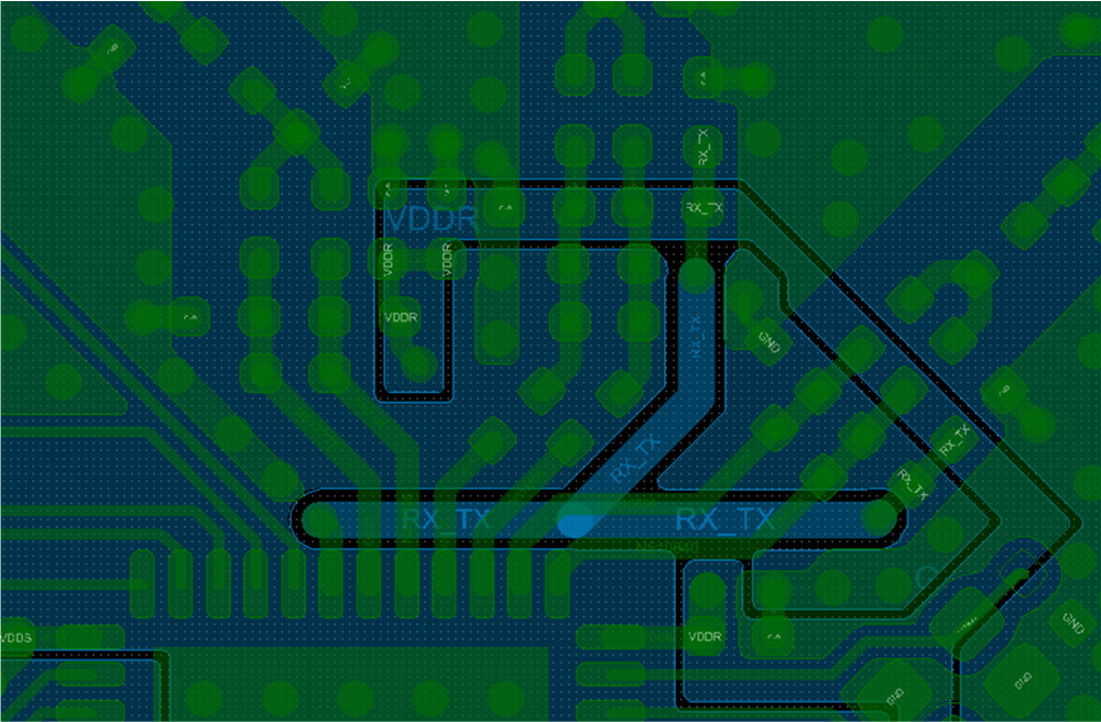
The two plots below show the layout. Figure 6-2 shows the layout of the full board used for testing. Figure 6-3 shows a zoomed in version showing the VDDR traces.
 Figure 6-2 CC1352PEM-XD7793-XD24-PA24_10dBm Layout, Full
 Figure 6-3 CC1352PEM-XD7793-XD24-PA24_10dBm Layout, Zoomed