SWRA729 April 2022 CC1352P , CC1354P10 , CC2652P
1.2.1 Component Placement and Layout
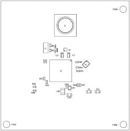
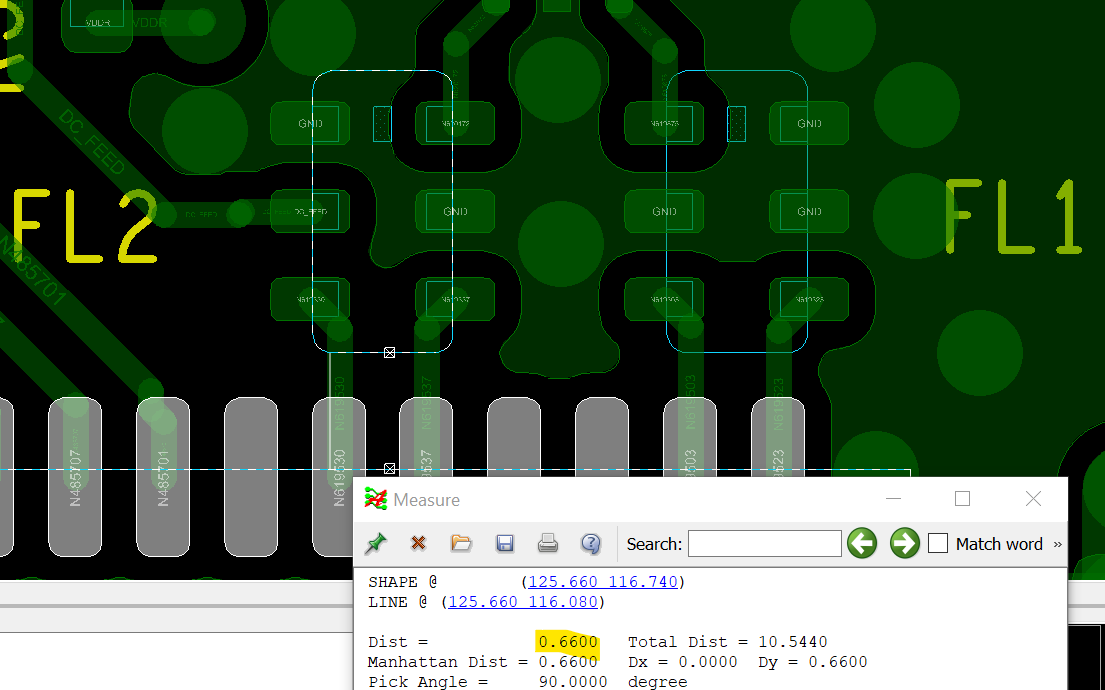
The PA IPC component placement influences the RF performance and the reference design should be followed as close as possible, refer to Figure 1-5 and Figure 1-6. The distance between the PA IPC and the CC1352P/CC2652P is important and this should be 0.66 mm as can be seen in Figure 1-6.
In the event that the reference design cannot be copied then the routing from the RF pins must be symmetrical to the IPC. The length of the tracks should be kept to a minimum and preferably the same recommended length that is used in the reference design of 0.66 mm. The width of the tracks between CC1352P/CC2652P and the IPC should also be kept as 0.15 mm.
If the recommended distance of 0.66 mm, 0.15 mm track width or GND via placements are too far away from the IPC, this will introduce phase shifts and additional parasitic inductance. Not following the reference design will affect the Tx output power, Tx harmonics and Rx sensitivity. Refer to Figure 1-6 for recommended GND via placements for the IPC.
All component ground pads should have the own ground via which should be positioned as close as possible to the ground pad. When positioning the ground vias for the component pad grounds it is important to try to keep the return path loop to ground as little as possible in order to prevent unnecessary radiated emissions.
The DC blocking capacitor and bypass capacitor is integrated into the PA IPC. U2 is a compact SPDT switch that combines the two RF ports into one common RF port.
 Figure 1-5 CC2652P Component Placement
 Figure 1-6 Via Placement and Distance between CC1352P / CC2652P and the PA IPC (FL2)