SWRU612 December 2023 CC3300 , CC3301 , CC3351
- 1
- Abstract
- Trademarks
- 1Introduction
-
2Schematic Considerations
- 2.1 Schematic Reference Design
- 2.2 Power Supply
- 2.3 Clock Source
- 2.4 Radio Frequency (RF)
- 2.5 Digital Interfaces
- 3Layout Considerations
3.3 Radio Frequency (RF)
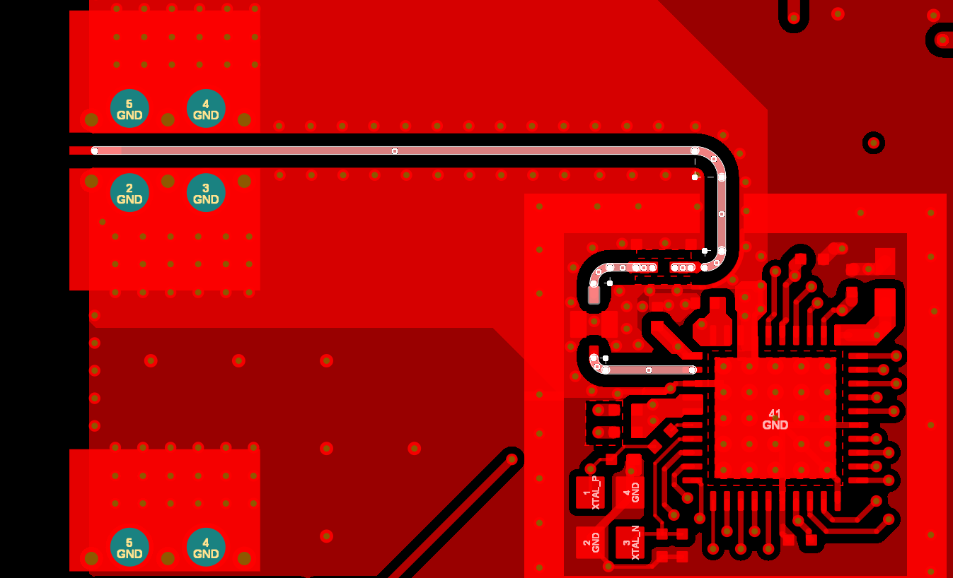
Figure 3-8 below shows the RF section as it appears on the reference design. Special care must be taken when designing this area of the layout in order to achieve peak performance. A poor layout can cause performance degradation for the output power, EVM, sensitivity, and spectral mask.
Figure 3-8 is sampled from the CC330x reference design files.
 Figure 3-8 Reference Design RF Path
In addtion to following the reference design as close as possible, please comply with the guidelines listed below.
- The RF trace should have a constant 50 Ω characteristic impedance. This is achieved by matching the CPWG based on the dielectric, layer stackup, ground plane spacing, and trace thickness. These parameters should be consistent throughout the length of the trace.
- The entire RF trace should only be on the top layer of the PCB, and the layer immediately underneath should be one constant ground plane (with the exception of the XTAL cutout) for the trace reference.
- The RF trace should be as clean and straight as possible with no components besides the band pass filter and matching filter before the antenna. This is to avoid unwanted component to component coupling. If a straight RF trace is not possible, rounded curves are acceptable.
- The RF trace should be as isolated as possible from other components to decrease noise. Ground planes should surround the RF trace, and distance between ground via stitching should be less than 1/8th of the minimum wavelength.
- The band pass filter should be as far as possible (within design space limits) from the RF_BG pin (pin 2) and the VDDA decoupling capacitors on pins 4 and 5.
- A ground via should be placed between the two ground pads for the band pass filter (BPF). The ground plane on both sides of the BPF should be connected to enable one common ground plane for the entire area. There should be increased ground via stitching in the ground plane between the BPF and the PA_LDO_OUT decoupling capacitor (pin 1).
- There should be no high frequency signal traces or test points close to the RF trace.
Another impactful factor in RF performance is the stackup. As an example, Table 3-1 contains the stackup (from top to bottom) used in the BP-CC3301 design.
| Layer | Name | Thickness | εr |
|---|---|---|---|
| Top Soldermask | |||
| Top Solder | 1.00 mil | 3.5 | |
| 1 | Top Layer | 1.85 mil | |
| Dielectric 1 | 5.48 mil | 4.2 | |
| 2 | L02_GND | 1.26 mil | |
| Dielectric 2 | 42.82 mil | 4.2 | |
| 3 | L03_PWR | 1.26 mil | |
| Dielectric 3 | 5.48 mil | 4.2 | |
| 4 | Bottom Layer | 1.85 mil | |
| Bottom Solder | 1.00 mil | 3.5 | |
| Bottom Soldermask |
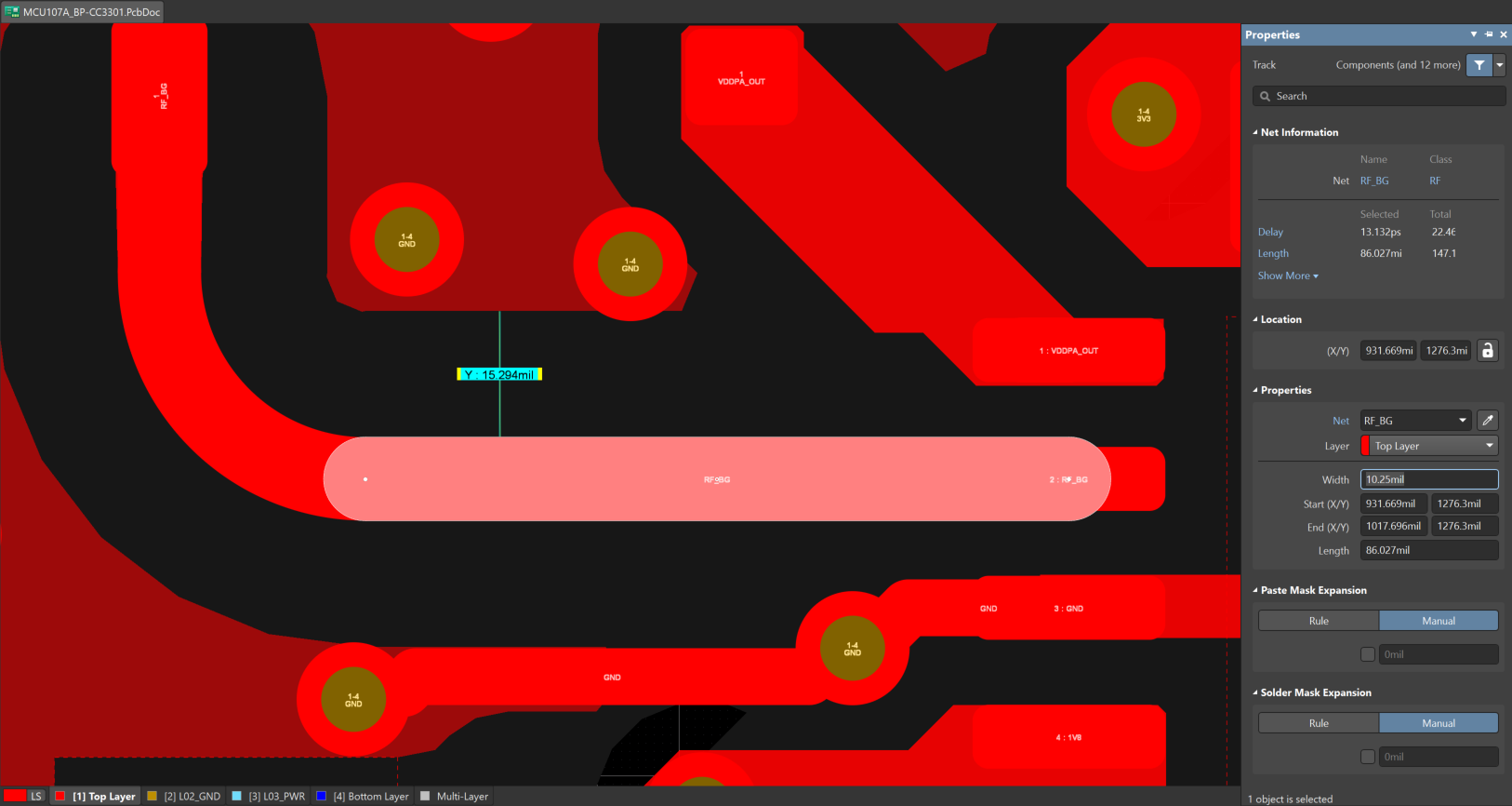
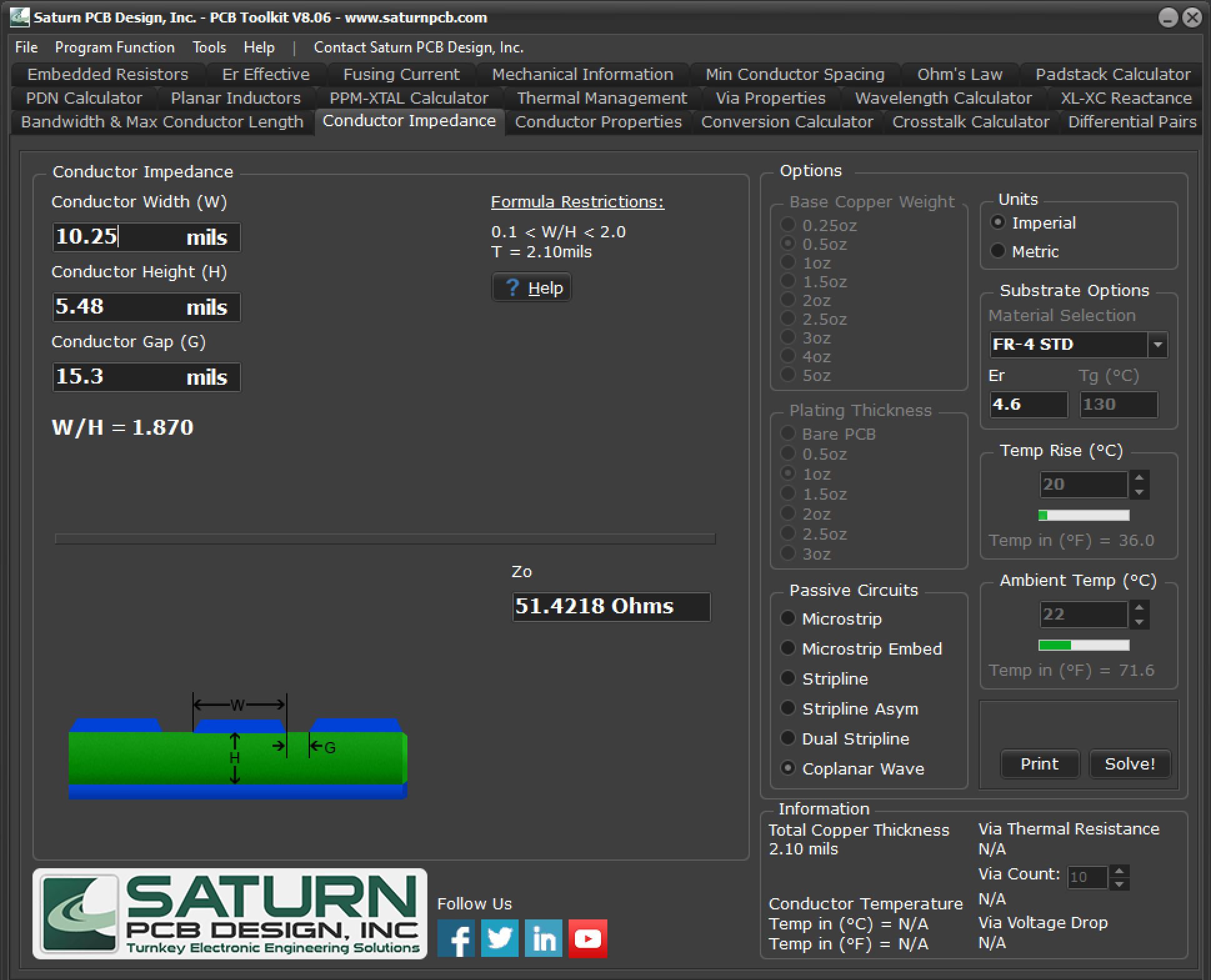
The RF signal from the device is routed to the antenna using a coplanar waveguide (CPW-G) structure. This structure offers the maximum isolation across the filter gap, and the best possible shielding to the RF lines. It is imperative to take in account the stackup and trace measurements in order to achieve a 50 ohm impedance. Figure 3-9 and Figure 3-10 illustrate examples of calculating trace impedance using the BP-CC3301 EVM as an example.
This image is sampled from the BP-CC3301 design files.
 Figure 3-9 Example of Taking RF Trace Measurements
 Figure 3-10 Example of Calculating Trace Impedance