SWRZ099B April 2020 – March 2022 AWR6843AOP
PACKAGE#02
Surface Wave Artifact from PCB
Revisions Affected
AWR6843AOP ES2.0
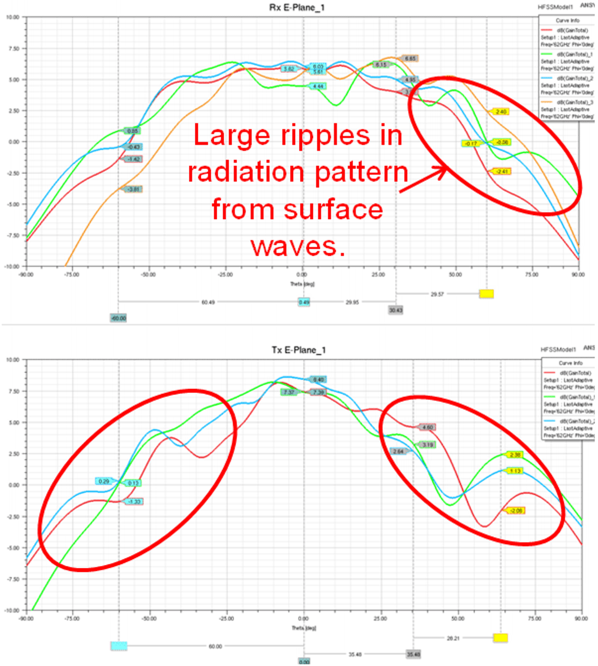
Description:
Large PCBs area around the E-plane causes surface waves that create large ripples in the elevation direction of the AoP antenna radiation pattern.
Workaround #1
Keep the Edge of PCB close to the edge of the AoP device in the E-plane to minimize the surface wave ripples.
 Figure 6-1 Small form factor board with PCB edge less than 0.3mm
Workaround #2
If a larger board is needed for the solution, a trapezoid cutout with the PCB edge less than <0.3mm from the edge of the AoP should be implemented to minimize the ripples caused by surface waves.
 Figure 6-2 Large form factor board with trapezoidal cutout and PCB edge less than
0.3mm
Figure 6-2 Large form factor board with trapezoidal cutout and PCB edge less than
0.3mm