TIDT277 April   2022


  1.   Description
  2.   Features
  3.   Applications
  4. 1Test Prerequisites
    1. 1.1 Voltage and Current Requirements
    2. 1.2 Considerations
    3. 1.3 Dimensions
  5. 2Testing and Results
    1. 2.1 Efficiency Graphs, all Outputs Similar Loaded
    2. 2.2 Load Regulation
    3. 2.3 Cross Regulation and Further Data For Non-Symmetrical Loading
    4. 2.4 Line Regulation at Full Load to all Outputs
    5. 2.5 Thermal Images
  6. 3Waveforms
    1. 3.1 Switching
      1. 3.1.1 Switchnode to GND
      2. 3.1.2 Diode D3
    2. 3.2 Output Voltage Ripple
    3. 3.3 Input Voltage Ripple
      1. 3.3.1 Power Stage Input
      2. 3.3.2 Between L1 and L2
      3. 3.3.3 Input Terminal
    4. 3.4 Start-Up Sequence
    5. 3.5 Shutdown Sequence

Shutdown Sequence

Shutdown behavior of channel U is shown in the following figure.

GUID-20220405-SS0I-BDDH-DMMB-LH7SCHWGXWXR-low.jpg

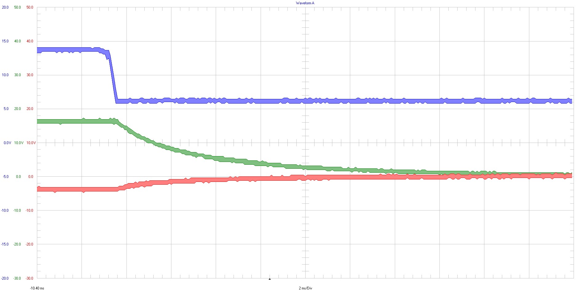
Ch1

Input voltage

5 V / div


Ch2

+17 VOUT

10 V / div


Ch3

-4 VOUT

10 V / div


20 MHz bandwidth

2 ms / div

Figure 3-9 Shutdown Channel U