TIDT286 June   2022


  1.   Description
  2.   Features
  3.   Applications
  4. 1Test Prerequisites
    1. 1.1 Voltage and Current Requirements
    2. 1.2 Considerations
    3. 1.3 Dimensions
  5. 2Testing and Results
    1. 2.1 Efficiency Graph
    2. 2.2 Loss Graph
    3. 2.3 Load Regulation
    4. 2.4 Line Regulation
    5. 2.5 Thermal Images
      1. 2.5.1 0.5-A Output Current
      2. 2.5.2 1-A Output Current
      3. 2.5.3 1.5-A Output Current
      4. 2.5.4 2-A Output Current
      5. 2.5.5 Pulsed Ouput Current
    6. 2.6 Bode Plots
      1. 2.6.1 6-V Input Voltage
      2. 2.6.2 12-V Input Voltage
  6. 3Waveforms
    1. 3.1 Switching
      1. 3.1.1 Transistor Q1
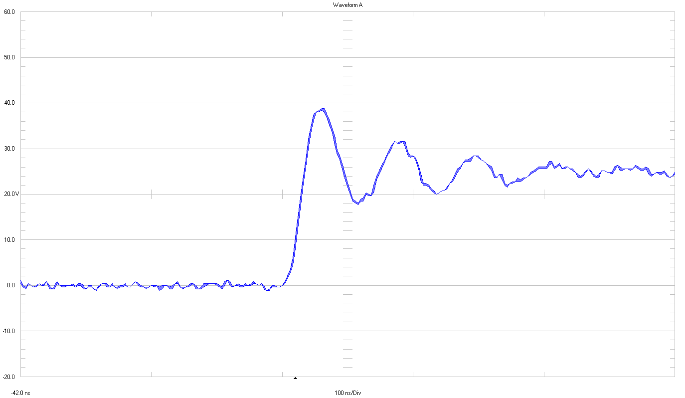
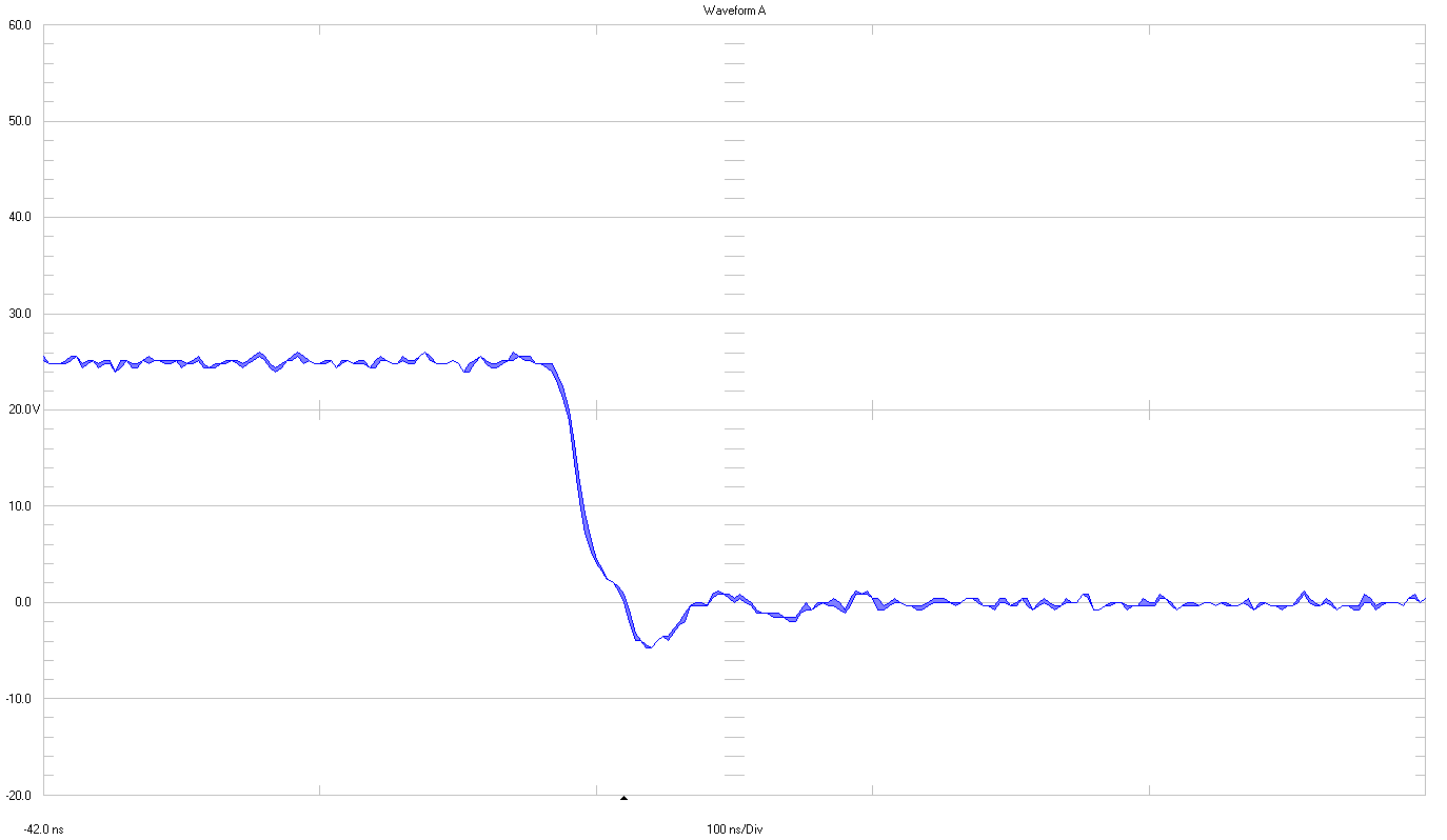
        1. 3.1.1.1 Drain - Source
        2. 3.1.1.2 Gate - Source
      2. 3.1.2 Diode D3
    2. 3.2 Input Voltage Ripple
      1. 3.2.1 20-MHz Bandwidth
      2. 3.2.2 Full Bandwidth
    3. 3.3 Output Voltage Ripple
    4. 3.4 Load Transients
      1. 3.4.1 Switching Load From 1 A to 2 A
      2. 3.4.2 Switching Load From 0.2 A to 2 A
        1. 3.4.2.1 50% Duty Cycle
        2. 3.4.2.2 Low Duty Cycle (TON = 3 ms; TOFF = 30 ms)
    5. 3.5 Start-Up Sequence
    6. 3.6 Shutdown Sequence

Drain - Source

GUID-20220524-SS0I-RGXW-W5RX-6ZQQ4KVPWNJX-low.png

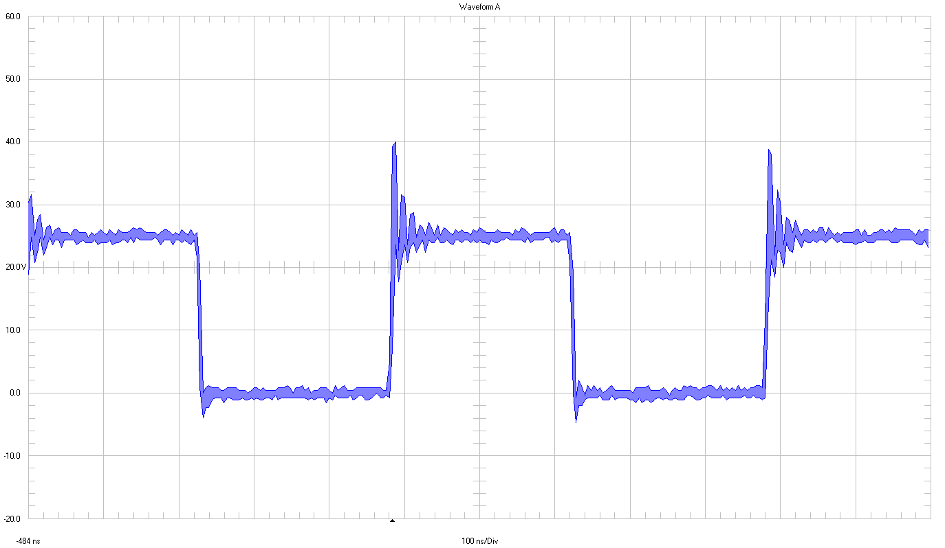
10 V / div

100 ns / div

full bandwidth

GUID-20220524-SS0I-FXZD-HPWT-GHXFWCW9LN17-low.png
GUID-20220524-SS0I-KXJ4-9BTZ-CFK0FDVNHJNS-low.png

10 V / div

100 ns full scale

full bandwidth

Figure 3-1 Waveform Q1 (Drain-Source)