TIDT313 November 2022
3.1 Switching
Switching behavior is shown in the following figures.
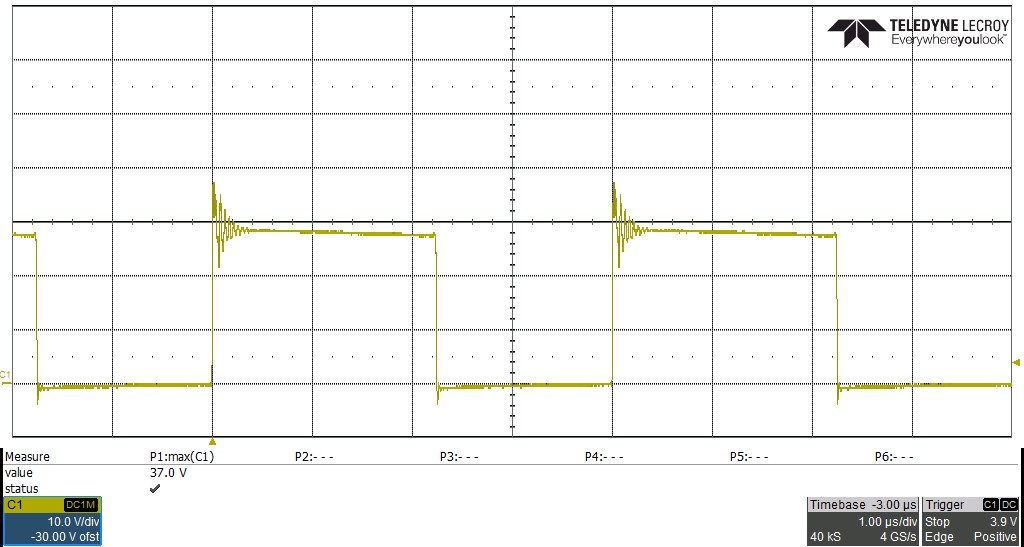 Figure 3-1 Voltage Drain-to-Source, Q6,
37-V Input, 3.3-A Load, Measured 37.0-V Vpeak
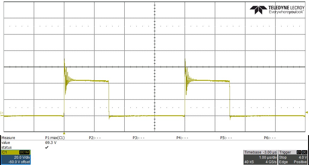 Figure 3-2 Voltage Drain-to-Source, Q6,
57-V Input, 3.3-A Load, Measured 69.3-V Vpeak
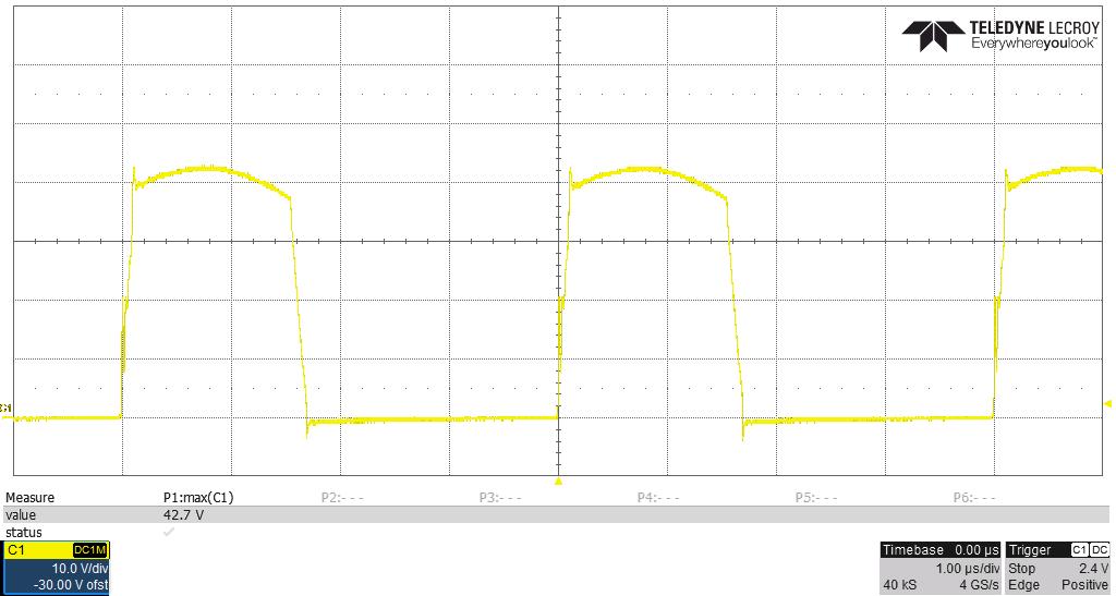 Figure 3-3 Voltage Drain-to-Source, Q8,
37-V Input, 3.3-A Load, Measured 42.7-V Vpeak
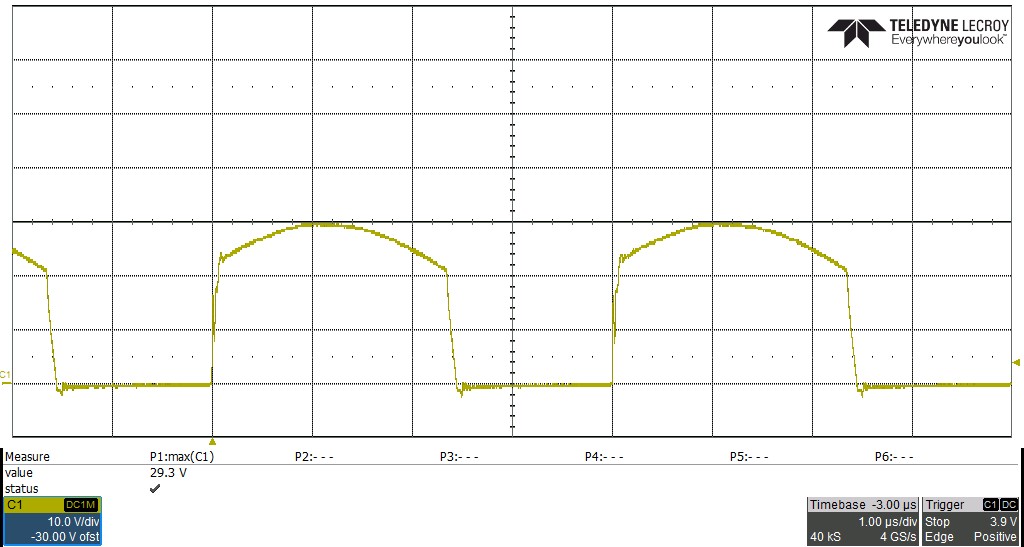 Figure 3-4 Voltage Drain-to-Source, Q8,
57-V Input, 3.3-A Load, Measured 29.3-V Vpeak
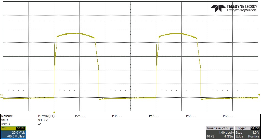 Figure 3-5 Voltage Drain-to-Source, Q10, 37-V Input, 3.3-A Load, Measured 93.3-V Vpeak
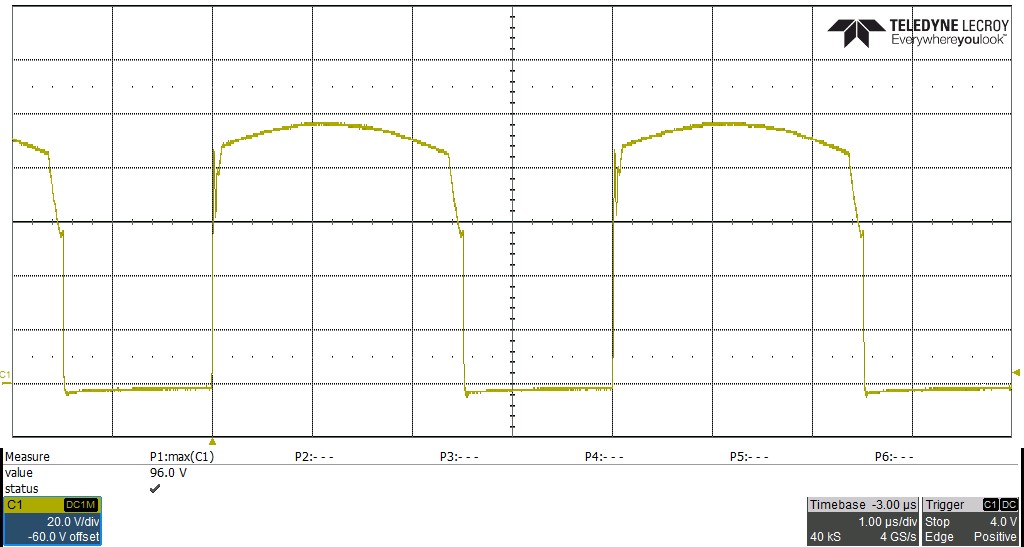 Figure 3-6 Voltage Drain-to-Source, Q10, 57-V Input, 3.3-A Load, Measured 96.0-V Vpeak