TIDT321 January   2023


  1.   Description
  2.   Features
  3.   Applications
  4. 1Test Prerequisites
    1. 1.1 Voltage and Current Requirements
    2. 1.2 Required Equipment
    3. 1.3 Dimensions
  5. 2Testing and Results
    1. 2.1 Efficiency and Load Regulation Graphs
    2. 2.2 Thermal Images
    3. 2.3 Bode Plots
  6. 3Waveforms
    1. 3.1 Switching
    2. 3.2 Output Voltage Ripple
    3. 3.3 Load Transients
    4. 3.4 Start-Up Sequence
    5. 3.5 Other Waveforms

Switching

Switching behavior is shown in the following figures.

The waveform in Figure 3-1 was created using the following conditions: input voltage = 630 VDC; output
power = full load.
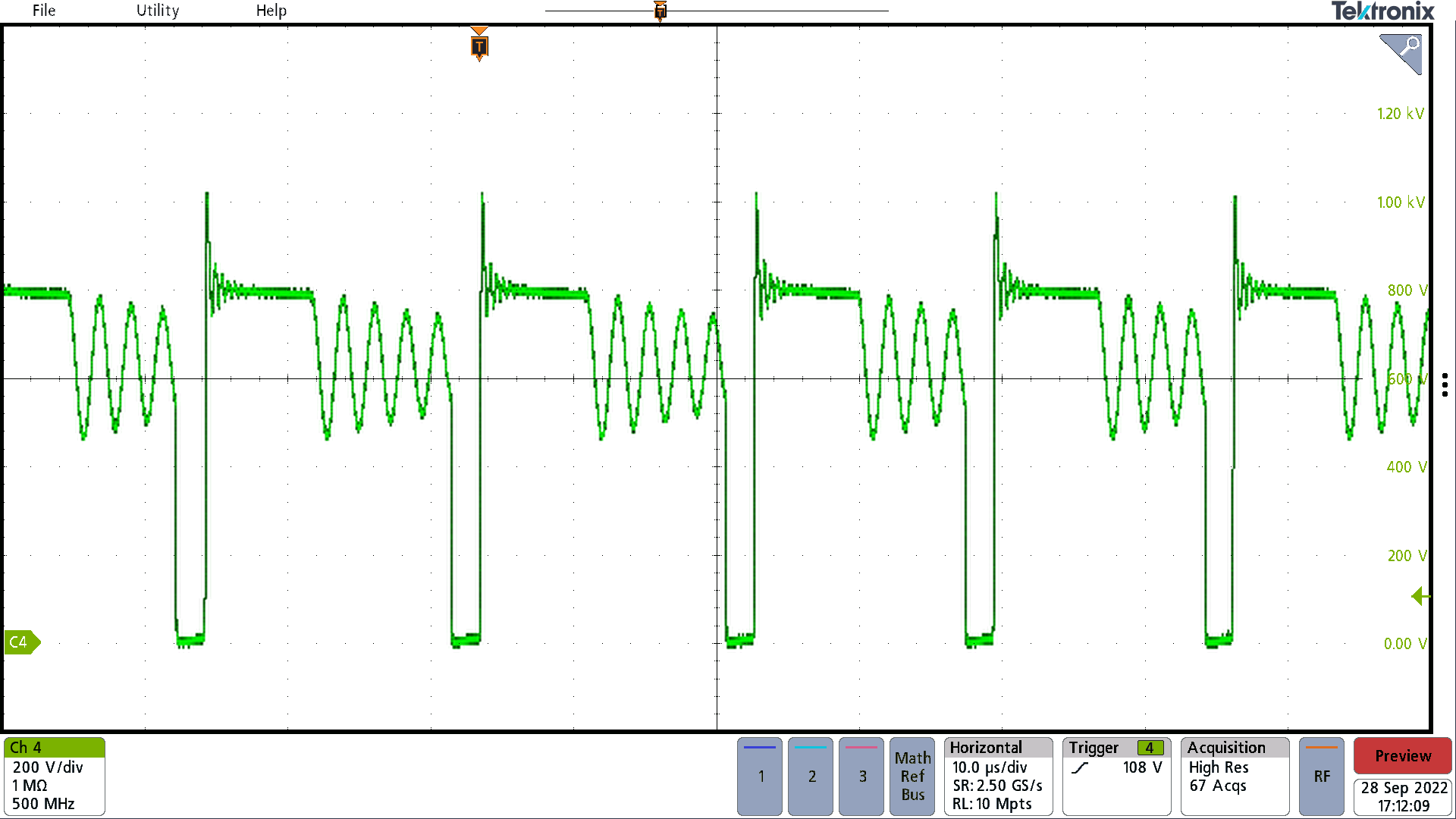
GUID-20221220-SS0I-FF3M-43GW-GSNTX9BH4PN6-low.png Figure 3-1 Switch Node

The waveform in Figure 3-2 was created using the following conditions: input voltage = 330 VDC; output
power = full load.
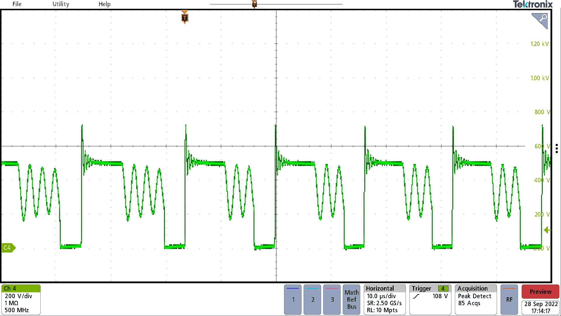
GUID-20221220-SS0I-WM68-FBBT-QWX66BL2ZH16-low.png Figure 3-2 Switch Node