TIDT335 july 2023
3.4 Load Step
Figure 3-7 through Figure 3-8 show the load step behavior waveforms of various devices.

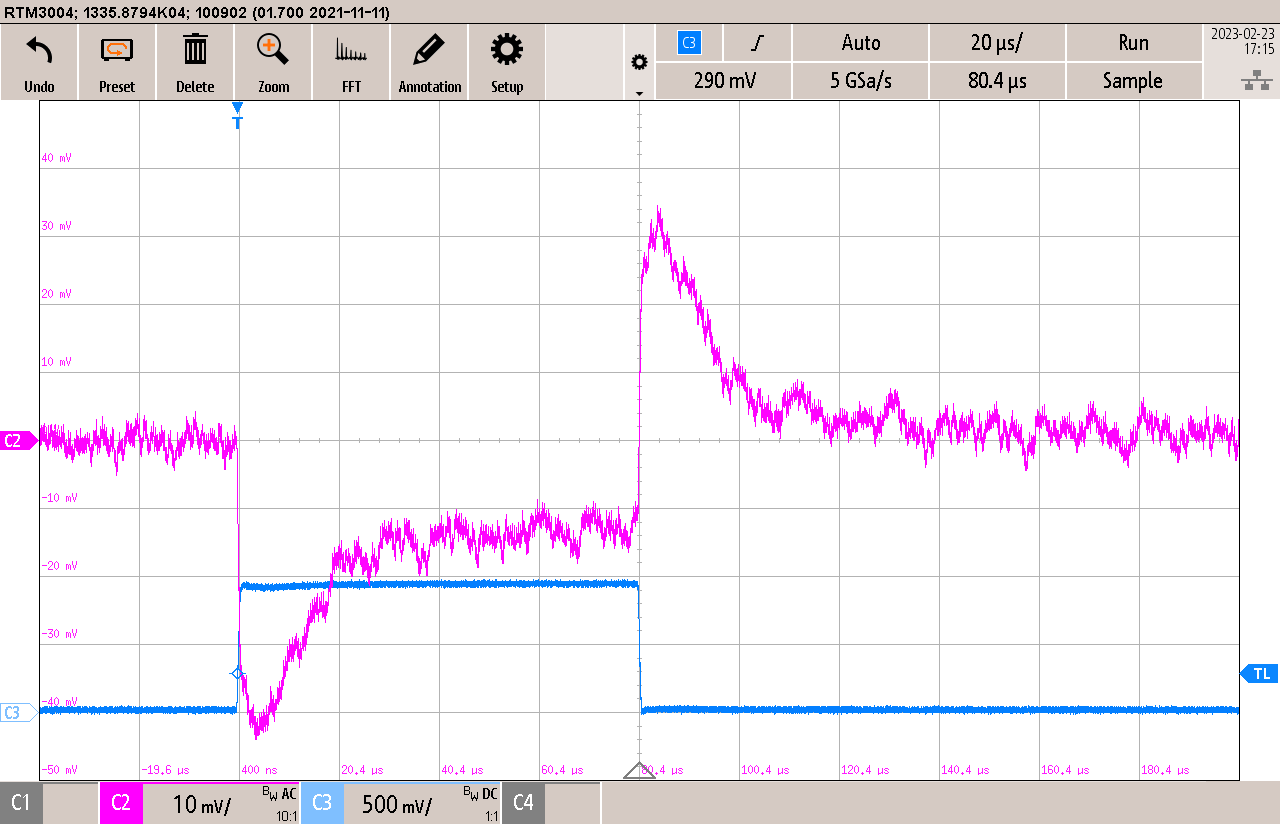
CH2: AC coupled output voltage, scale: 10
mV/div, 20 µs/div, 20-MHz bandwidth
CH3: Output current, scale: 1 A/div, 20 µs/div, 20-MHz bandwidth, 2 A offset: 0 V = 2 A
Figure 3-6 TPS62810-Q1 Load Step Behavior, 2 A to
4 ACH3: Output current, scale: 1 A/div, 20 µs/div, 20-MHz bandwidth, 2 A offset: 0 V = 2 A

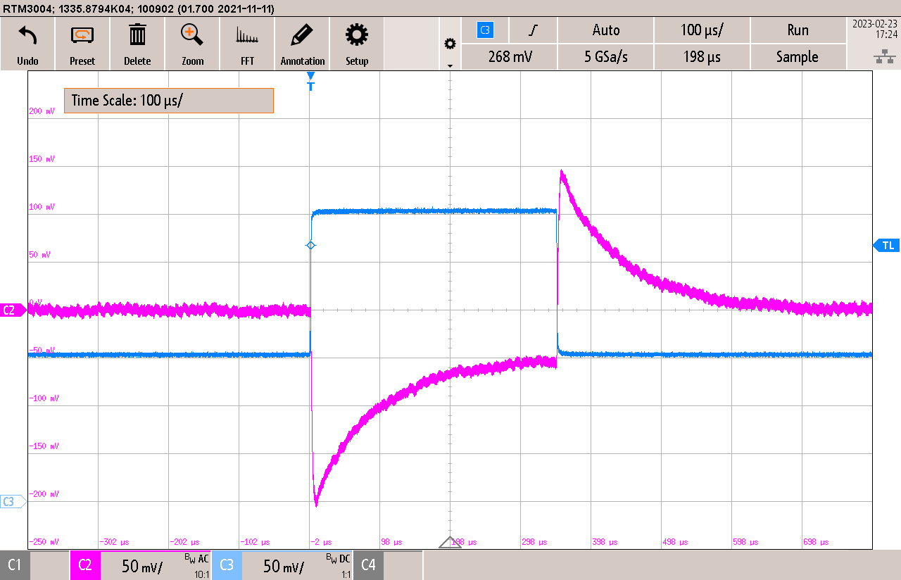
CH2: AC coupled output voltage, scale: 50
mV/div, 100 µs/div, 20-MHz bandwidth
CH3: Output current, scale: 300 mA/div, 100 µs/div, 200-MHz bandwidth
Figure 3-7 LMR43620-Q1 Load Step Behavior, 300 mA
to 600 mACH3: Output current, scale: 300 mA/div, 100 µs/div, 200-MHz bandwidth

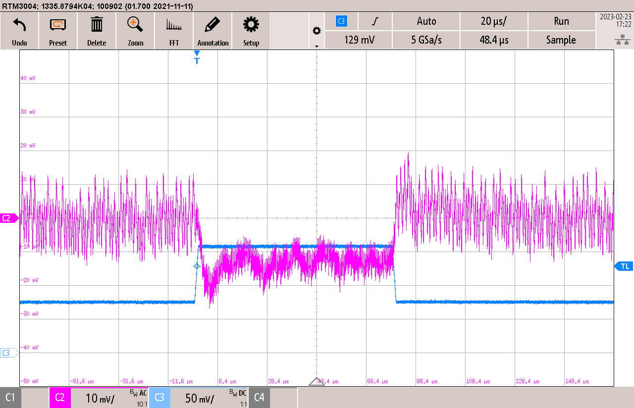
CH2: AC coupled output voltage, scale: 10
mV/div, 20 µs/div, 20-MHz bandwidth
CH3: Output current, scale: 100 mA/div, 20 µs/div, 20-MHz bandwidth
Figure 3-8 TPS62850-Q1 Load Step Behavior, 150 mA
to 300 mACH3: Output current, scale: 100 mA/div, 20 µs/div, 20-MHz bandwidth