TIDT336 may   2023


  1.   1
  2.   Description
  3.   Features
  4.   Applications
  5. 1Test Prerequisites
    1. 1.1 Voltage and Current Requirements
    2. 1.2 Required Equipment
    3. 1.3 Considerations
    4. 1.4 Dimensions
    5. 1.5 Test Setup
  6. 2Testing and Results
    1. 2.1 Efficiency Graph
    2. 2.2 Efficiency Data
    3. 2.3 Static Output Voltage Variation vs Load Current and VIN
      1. 2.3.1 24-V Output Voltage
      2. 2.3.2 3.3-V Output Voltage
      3. 2.3.3 U2 Input Voltage
  7. 3Waveforms
    1. 3.1 Switching Waveforms on Pin 1 of U1 (SW), Anodes of D1 and D4, at Full Load
      1. 3.1.1 18-V Input Voltage
      2. 3.1.2 24-V Input Voltage
      3. 3.1.3 32-V Input Voltage
    2. 3.2 Output Voltage Ripple
    3. 3.3 Load Transients
    4. 3.4 Start-Up Sequence
      1. 3.4.1 No Load
      2. 3.4.2 Full Load
    5. 3.5 Shutdown Sequence

Load Transients

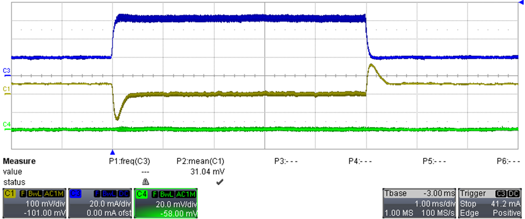
During load transients, the outputs of the board were measured by supplying the converter at 24 VDC while the load on 24 VOUT was switched between 20 mA and 60 mA; the load on 3.3 VOUT was constant at 15 mA. For all waveforms the bandwidth limit of the oscilloscope was set to 20 MHz.

GUID-20230511-SS0I-KXSR-M47Q-FQNF9ZK9DWLB-low.png

C1: 24 VOUT

(100 mV / div)


C3: IOUT 24 VOUT

(20 mV / div)


C4: 3.3 VOUT

(20 mV / div)


1 ms / div)

Figure 3-6 Load Transient