TIDT360 November 2023
3.1 Switching
Switching behavior is shown in the following figures.
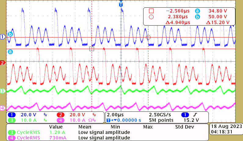
Phase 1 VSW and IL (CH1, CH3), Phase 2
VSW and IL (CH2, CH4)
Figure 3-1 Switch Node Voltages and
Inductor Currents of Main Boost Stage, at Iload = 0 A, VIN
= 12 V, VOUT = 45 V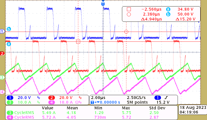
Phase 1 VSW and IL (CH1, CH3), Phase 2
VSW and IL (CH2, CH4)
Figure 3-2 Switch Node Voltages and
Inductor Currents of Main Boost Stage, at Iload = 2 A, VIN
= 12 V, VOUT = 45 V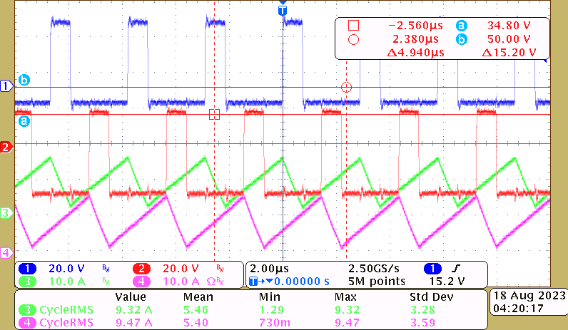
Phase 1 VSW and IL (CH1, CH3), Phase 2
VSW and IL (CH2, CH4)
Figure 3-3 Switch Node Voltages and
Inductor Currents of Main Boost Stage, at Iload = 4 A, VIN
= 12 V, VOUT = 45 V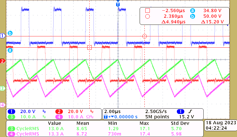
Phase 1 VSW and IL (CH1, CH3), Phase 2
VSW and IL (CH2, CH4)
Figure 3-4 Switch Node Voltages and
Inductor Currents of Main Boost Stage, at Iload = 6 A, VIN
= 12 V, VOUT = 45 V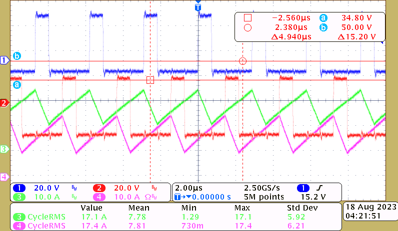
Phase 1 VSW and IL (CH1, CH3), Phase 2
VSW and IL (CH2, CH4)
Figure 3-5 Switch Node Voltages and
Inductor Currents of Main Boost Stage, at Iload = 8 A, VIN
= 12 V, VOUT = 45 V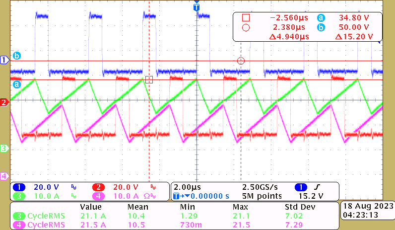
Phase 1 VSW and IL (CH1, CH3), Phase 2
VSW and IL (CH2, CH4)
Figure 3-6 Switch Node Voltages and
Inductor Currents of Main Boost Stage, at Iload = 10 A,
VIN = 12 V, VOUT = 45 V