TIDU858C March   2015  – May 2021


  1.   Description
  2.   Resources
  3.   Features
  4.   Applications
  5.   5
  6. 1System Description
    1. 1.1 Binary Inputs or Digital Inputs
      1. 1.1.1 Binary Input Application Functionality
      2.      Common Specifications
    2. 1.2 Approaches to Binary Input Module Design
      1. 1.2.1 ADC Versus MCU Based Binary Input Module (BIM)
    3. 1.3 Measurement of Wide Inputs With Programmable Thresholds
  7. 2Design Features
    1. 2.1 Electrical Specifications
    2. 2.2 Block Diagram
      1. 2.2.1 Analog-to-Digital Converter (ADC)
        1. 2.2.1.1 ADS795x SAR ADC Family
      2. 2.2.2 Protection and Signal Conditioning
      3. 2.2.3 Digital Isolator
        1. 2.2.3.1 Host (SPI) Interfacing Using the ISO6741
      4. 2.2.4 DC Power Supply Isolator
      5. 2.2.5 Design Alternative: ADC With Digitally Programmable Threshold
        1. 2.2.5.1 ADS7128 SAR ADC With Programmable Threshold
        2. 2.2.5.2 I2C Interfacing Using the ISO1640 and Optional Altert Interface Using ISO7710
  8. 3Circuit Design and Component Selection
    1. 3.1 Analog-to-Digital Converter (ADC)
    2. 3.2 Input Signal Conditioning
      1. 3.2.1 Voltage Divider
      2. 3.2.2 TLV6002 Operational Amplifier
    3. 3.3 Isolated Interface
    4. 3.4 Isolated DC Power Supply
      1. 3.4.1 Reinforced Power Isolator: UCC12050 High-Efficiency 500-mW DC/DC Converter
    5. 3.5 Enhancements
  9. 4Testing
    1. 4.1 Test Setup and Connection Diagram
    2. 4.2 Test Data
      1. 4.2.1 Voltage Measurement Accuracy Testing
    3. 4.3 Test Results Summary
  10. 5Design Files
    1. 5.1 Schematics
    2. 5.2 Bill of Materials
    3. 5.3 Altium Project
    4. 5.4 Gerber Files
  11. 6References
  12.   Trademarks
  13. 7About the Author
  14. 8Revision History

Test Setup and Connection Diagram

The setup shown in Figure 4-1 consists of a DC supply with current limit used for accurately powering the TIDA-00420 board. The DC supply is also used as a programmable voltage source for testing the measurement accuracy of captured samples of the interface board. The board is interfaced to the GUI for processing the samples and configuring the ADC.

GUID-20210407-CA0I-WPQ8-HFSV-M8M4M68RSPMR-low.gif Figure 4-1 Test Setup Layout

Figure 4-2 shows the connection diagram used for board testing. Connectors are provided to connect the AC or DC voltage inputs. Screw type terminals are provided to connect the DC supply communication interface connector (header-male type) to the ADC, and then to the host.
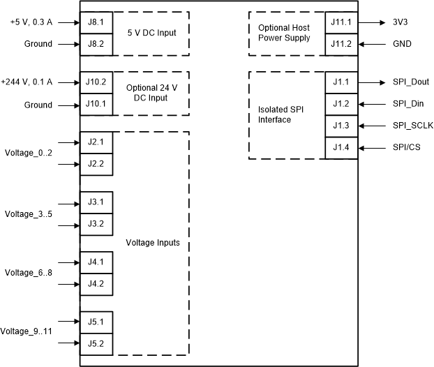
GUID-20210407-CA0I-QKX5-D0LL-GGSFDCZ0HMJZ-low.gif Figure 4-2 Connections for Performance Testing