TIDUEP0 May 2020
- Description
- Resources
- Features
- Applications
- 1Design Images
- 2System Description
-
3System Overview
- 3.1 Block Diagram
- 3.2 Design Considerations
- 3.3
Highlighted Products
- 3.3.1 TPD4E05U06 4-Channel Ultra-Low-Capacitance IEC ESD Protection Diode
- 3.3.2 TPD2EUSB30 2-Channel ESD Solution for SuperSpeed USB 3.0 Interface
- 3.3.3 2.3.3 HD3SS3220 10Gbps USB 3.1 USB Type-C 2:1 MUX With DRP Controller
- 3.3.4 TPS54218 2.95V to 6V Input, 2A Synchronous Step-Down SWIFT™ Converter
- 3.3.5 TPS54318 2.95V to 6V Input, 3A Synchronous Step-Down SWIFT™ Converter
- 3.3.6 CSD19538Q3A 100V, N ch NexFET MOSFET™, single SON3x3, 49mOhm
- 3.3.7 LM3488 2.97V to 40V Wide Vin Low-Side N-Channel Controller for Switching Regulators
- 3.3.8 TPS61178 20-V Fully Integrated Sync Boost with Load Disconnect
- 3.3.9 LMZM23601 36-V, 1-A Step-Down DC-DC Power Module in 3.8-mm × 3-mm Package
- 3.3.10 TPS7A39 Dual, 150mA, Wide-Vin, Positive and Negative Low-Dropout (LDO) Voltage Regulator
- 3.3.11 TPS74201 Single-output 1.5-A LDO regulator, adjustable (0.8V to 3.3V), any or no cap, programmable soft start
- 3.3.12 LP5910 300-mA low-noise low-IQ low-dropout (LDO) linear regulator
- 3.3.13 LP5907 250-mA ultra-low-noise low-IQ low-dropout (LDO) linear
- 3.3.14 INA231 28V, 16-bit, i2c output current/voltage/power monitor w/alert in wcsp
- 3.4
System Design Theory
- 3.4.1 Input Section
- 3.4.2
Designing of SEPIC based High Voltage Supply
- 3.4.2.1 Basic Operation Principle of SEPIC Converter
- 3.4.2.2 Design of Dual SEPIC Supply using uncoupled inductors
- 3.4.2.3 Duty Cycle
- 3.4.2.4 Inductor Selection
- 3.4.2.5 Power MOSFET Selection
- 3.4.2.6 Output Diode Selection
- 3.4.2.7 Coupling Capacitor Selection
- 3.4.2.8 Output Capacitor Selection
- 3.4.2.9 Input Capacitor Selection
- 3.4.2.10 Programming the Output Voltage
- 3.4.3 Designing the Low Voltage Power Supply
- 3.4.4 Designing the TPS54218 through Webench Power Designer
- 3.4.5 ± 5V Transmit Supply Generation
- 3.4.6 System Clock Synchronization
- 3.4.7 Power and data output connector
- 3.4.8 System Current and Power Monitoring
- 4Hardware, Software, Testing Requirements, and Test Results
- 5Layout Guidelines
- 6Design Files
- 7Software Files
- 8Related Documentation
- 9About the Author
3.4.4 Designing the TPS54218 through Webench Power Designer

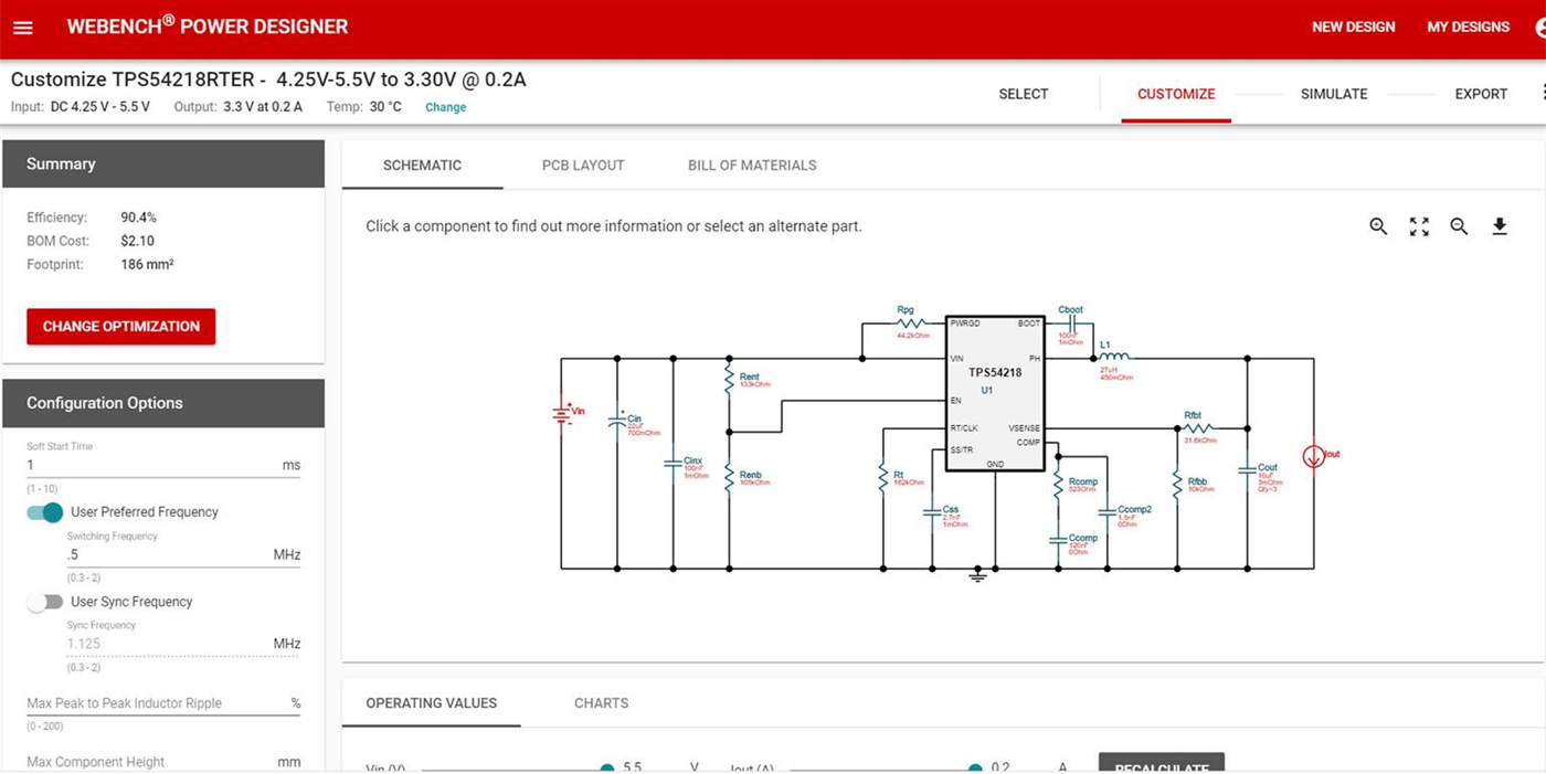
The Figure 12 shows a Webench design used to evaluate the TPS54218 with an output voltage of 3.3 V at 200mA. Webench Power Designer tool allows the user to simulate real time data for the product selected (efficiency, transient response, startup, etc.) and a capability to export Altium files to complete a board design.
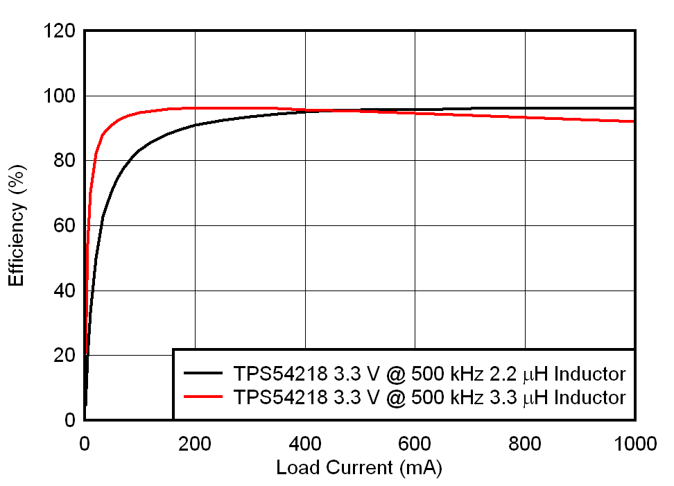
For the ultrasound power supply design, the TPS54218 was selected to power the low voltage for the FPGA and the AFE5832LP. Since the size of the total solution was a concern, a module was considered. Comparing the difference between a power module and a dc/dc converter (internal inductor vs external inductor), the total system efficiency was evaluated. The DC/DC converter solution (TPS54218) allowed for more flexibility by increasing the inductor value, which led to an increase in efficiency (see Figure 14 in Power Measurement section).
When comparing how different inductor values effect the efficiency of a buck converter, the TPS54218 was evaluated with two different inductor values. In Figure 13, the TPS54218 efficiency was tested for two different inductor values (2.2uH vs 33uH) using a load generator. For light load conditions, the 33uH inductor had a much higher efficiency when compared to the 2.2uH solution. This is due to the AC conduction losses of the inductor which decrease the efficiency of the solution. Moving forward for the the low voltage power supply design, a 33uH inductor was chosen to improve the efficiency.


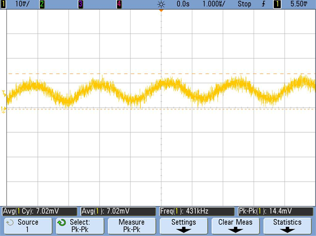
Figure 14 shows the 2 V supply output voltage ripple of the TPS54218. The measured Pk-Pk ripple was measured at 14.4mV. The remaining low voltage power supplies all had an output voltage ripple of less than 10m V.