TIDUEZ0A March   2021  – March 2022 TMS320F28P550SJ , TMS320F28P559SJ-Q1


  1.   Description
  2.   Resources
  3.   Features
  4.   Applications
  5.   5
  6. 1System Description
    1. 1.1 Key System Specifications
  7. 2System Overview
    1. 2.1 Block Diagram
    2. 2.2 Design Considerations
      1. 2.2.1 Three-Phase ANPC Inverter Architecture Overview
      2. 2.2.2 LCL Filter Design
      3. 2.2.3 Power Switching Devices Selection
      4. 2.2.4 GaN Power Stage
      5. 2.2.5 Voltage Sensing
      6. 2.2.6 Current Sensing
      7. 2.2.7 System Power Supplies
        1. 2.2.7.1 Isolated Bias Supplies
      8. 2.2.8 Si Gate Driver Circuit
  8. 3Hardware, Software, Testing Requirements, and Test Results
    1. 3.1 Hardware and Software Requirements
      1. 3.1.1 Hardware
      2. 3.1.2 Software
    2. 3.2 Testing TIDA-010210 With AC Resistive Load
      1. 3.2.1 Test Setup
      2. 3.2.2 Experimental Results
    3. 3.3 Testing TIDA-010210 in PFC Operation
      1. 3.3.1 Test Setup
      2. 3.3.2 Experimental Results
  9. 4Design and Documentation Support
    1. 4.1 Design Files
      1. 4.1.1 Schematics
      2. 4.1.2 BOM
      3. 4.1.3 Altium Project
      4. 4.1.4 Gerber Files
      5. 4.1.5 Assembly Drawings
    2. 4.2 Tools and Software
    3. 4.3 Support Resources
    4. 4.4 Trademarks
  10. 5About the Authors
  11. 6Revision History

Si Gate Driver Circuit

Figure 2-15 shows the schematic of the isolated Si MOSFET gate driver. As the UCC21541 gate driver used has two isolated gate drive outputs, it can drive both the devices in the half-bridge power stage of the power board. The drive current is controlled separately for turn-on and turn-off with diode controlled separate drive paths. A ferrite bead is used in the gate drive path to suppress ringing.
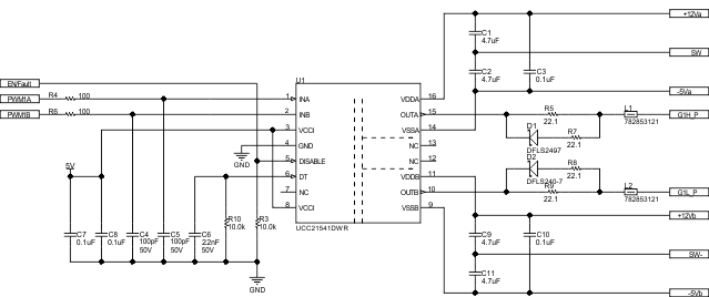
GUID-20210218-CA0I-CXDK-DQVQ-WBTDNCF5LXFM-low.gif Figure 2-15 UCC21541 Gate Drive Circuit