TIDUF06 August 2022
- Description
- Resources
- Features
- Applications
- 5
- 1System Description
- 2System Overview
- 3Hardware, Testing Requirements, and Test Results
- 4Design Files
- 5Related Documentation
- 6Trademarks
1 System Description
Many automotive applications require small form factors that enable compact, modular, and remote systems. The growing demand for automotive vision systems also requires the flexibility of system components to meet the requirements of various image sensors to reduce the camera module design cycle and time-to-market. This reference design addresses these challenges by including a 2.9-megapixel imager, 4-Gbps serializer, and four-channel PMIC within two 20-mm x 20-mm circuit boards. The only connection required by the system is a single 50-Ω coaxial (coax) cable.
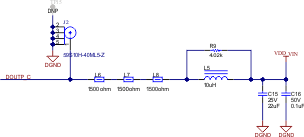
DC power, the FPD-Link front-channel, and the FPD-Link back-channel enter the board through the FAKRA coax connector. The POC filter in Figure 1-1 blocks all of the high-speed content of the signal (without significant attenuation) while allowing the DC (power) portion of the signal to pass through inductor L5.
 Figure 1-1 POC Filter Schematic
The DC portion is connected to the input of the TPS650330-Q1 PMIC. A dedicated mid-voltage buck regulator converts this to an intermediate 3.8 V. The two low-voltage buck regulators provide a dedicated 1.1 V for the imager and a dedicated 1.8 V shared by both the imager and serializer. An integrated high-PSRR, low-noise LDO provides a clean 3.3 V analog supply for the imager. The high-frequency portion of the signal is connected directly to the serializer. This is the path that the video data and control backchannel take between the serializer and deserializer.
The output of the imager is connected through a 4-lane MIPI CSI-2 interface to the serializer. The serializer transmits this video data over a single LVDS pair to the deserializer located on the other end of the coax cable.
Additionally, on the same coax cable, there is a separate low-latency, bidirectional control channel that provides the additional function of transmitting control information from an I2C port. This control channel is independent of the video blanking period. It is used by the system microprocessor to configure and control the imager.