SLLA557 June 2021 ISO1640 , ISOS141-SEP
Application Brief
Design Goals
|
Parameter |
Design Requirement |
|---|---|
| Supply voltage | 3.3 V |
| Signaling Rate | 1Mbps (fast Mode) |
| Maximum Total Ionizing Dose | 30krad(Si) |
| Maximum SEL to LET | 43MeV × cm2/mg |
| Isolation voltage | 3000 VRMS per UL1577 |
Design Description
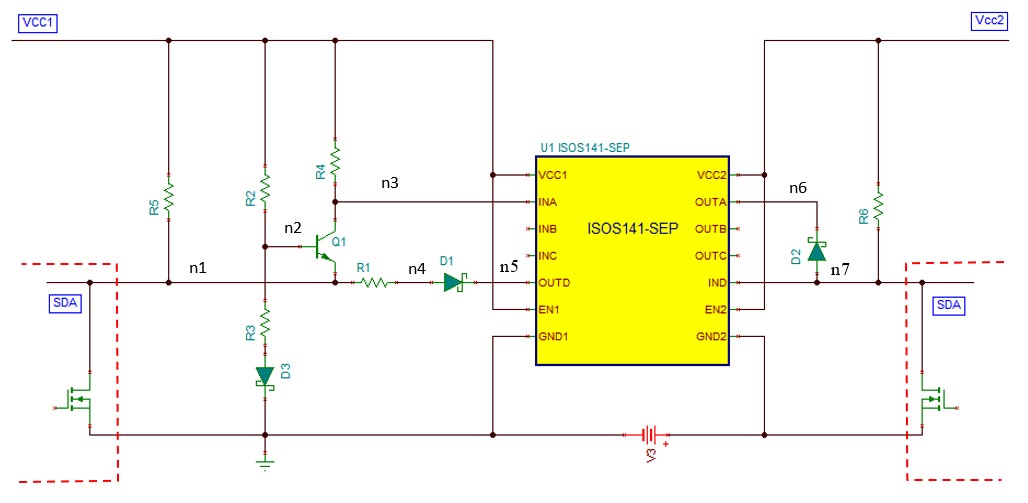
In spacecraft, I2C buses might be used for board-to-board communication, and the prevalence of using cold spares might require the addition isolation into the system. The I2C bus is a commonly-used bus for communication. The particular challenge in designing an isolated I2C interface by using standard digital isolators lies in the different operation modes between the two. The I2C bus operates in bidirectional, half-duplex mode, while standard digital isolators are unidirectional devices. To make efficient use of one technology supporting the other, external circuitry is required to separate the bidirectional bus into two unidirectional signal paths without introducing significant propagation delay.
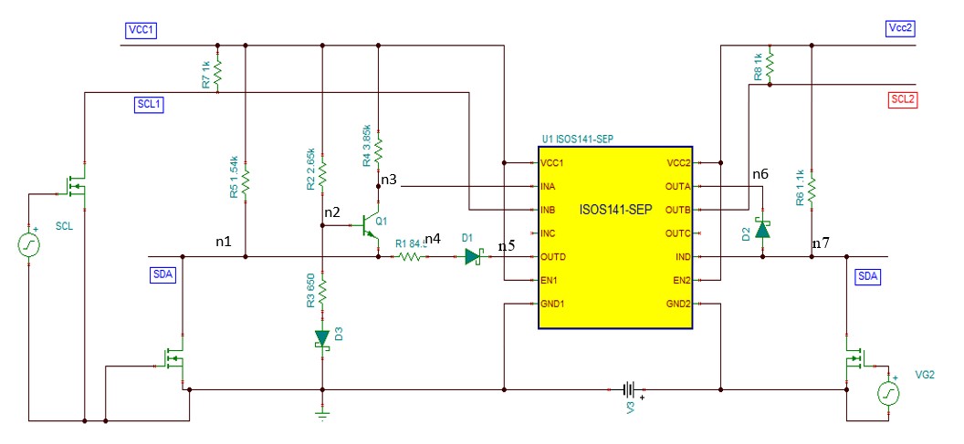
This circuit design uses an NPN transistor, 3 Schottky diodes, and 4 resistors to transform a digital isolator into an isolated I2C device.
Design Notes
Transistor Q1 and its surrounding resistor network provide the comparator function. Since the dominant switching level in I2C is logic low, the base of Q1 is so biased that a low level applied to n1 turns the transistor on, and a low level at n7 keeps Q1 at high impedance. While the R3, R2 voltage divider primarily determines the biasing, diode D3 provides temperature compensation. To prevent low level at n7 and thus n1 from turning Q1 on, the voltage level at n1 is raised by a voltage drop across R1 from n4, which raises the emitter potential of Q1, VE, and decreases the base-emitter voltage below the minimum turn-on level. However, care must be taken to maintain VE below the minimum input high-level threshold of SDA, which the I2C specification lists as VILmax = 0.3 × VCC.
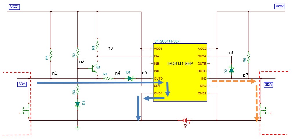
When the I2C bus at n7 is pulled to logic low state as illustrated in the dotted orange arrows in the next figure, the low state passing into IND and causes OUTD to go to low state. The voltage at n1 is pulled down to a low state illustrated by the blue arrows. The R1 introduces a voltage drop to n4 from n1, which raises the voltage at n1 high enough to turn off the Q1 but well below VILmax, thus presenting a valid low for an I2C input. At the same time, R4 provides a logic high at to the isolator input INA and causes OUTA to go high, preventing diode D2 from conducting.
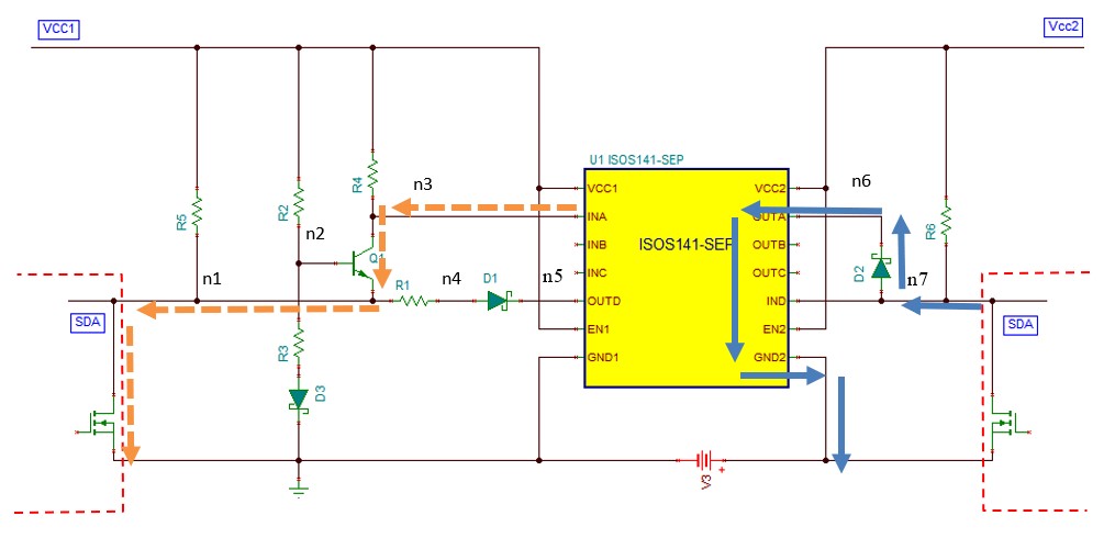
When n1 is pulled to a low state, the voltage across n2 and n1 is significantly lower than VE and causes Q1 to conduct. This causes the INA to go to a logic low illustrated by the dotted orange arrows in the next figure. The low-state signal passing through the isolator and causes OUTA to go low. The voltage at n7 is pulled down through the forward bias of diode D2 illustrated by the blue arrows. However, when n1 goes high, its voltage cannot return to the level of VCC1 immediately due to the remaining low-level signal at n7 and n5 that causes D1 to forward bias. Instead, n1 rises to the necessary VE potential that blocks Q1. It remains at this level until a high impedance across Q1 allows R4 to provide a logic high to the isolator input INA, thus releasing n6 and D3 and causing n7 to go high level. Only then will n1 be able to return to the level of VCC1.
Design Steps
- Calculate pullup resistors
See the I2C Bus Pullup Resistor Calculation application report for the equation to calculate the pullup resistor for n1 and n7. In this design, the calculated pullup resistors for both n1 and n7 are 1.1kΩ. The pullup resistances vary from the selected I2C devices and bus capacitance.
Notes:
- Include the capacitance of D1 and Q1 in the bus capacitance for n1 pullup resistor calculation
- Include the capacitance of D3 in the bus capacitance for n7 pullup resistor calculation
- Calculate R6 = pullup resistor for n7
R6 = 1.1kΩ - Calculate R5 and R4
R5 is parallel to R4. Assuming the transistor capacitance is 2.5 times smaller than the bus capacitance, we set R4 = 2.5 × R5 to make R5 have 2.5 times stronger pullup strength.R4 = 2.5R5 →(2)
Using (2) in (1)
Let RT = 1.1kΩ from n1 pullup resistor, R5 = 1.54kΩ and R4 = 3.85kΩ
- Calculate R2 and R3
R2 and R3 is a voltage divider that sets the bias voltage for transistor Q1. The bias voltage should be higher than the turn-off voltage of the transistor Q1, 0.6V, but lower than the SDA VILmax = 0.3 × VCC. The constant current through R2 and R3 must be less than 1mA.For VCC = 3.3V, 0.6V < bias voltage < 0.99V, let bias voltage = 0.65V
R3 = 650 Ω and R2 = 2.65kΩ
- Calculate R1
The purpose of R1 is to prevent transistor Q1 from turning on when n4 is pulled to 0V. The transistor Q1 turn-on voltage is 0.6 V, and the bias voltage is 0.65 V. Hence, the drop-out voltage across the R1 should be greater than the bias voltage minus the turn-on voltage but less than the VILmax. Also, the voltage drop across R1 is the voltage divider of R1 and R5Let the voltage-drop across R1 to be 0.17 V:
Using R5 = 1.54kΩ from the previous equation, R1 = 84.5Ω.
Design Simulations
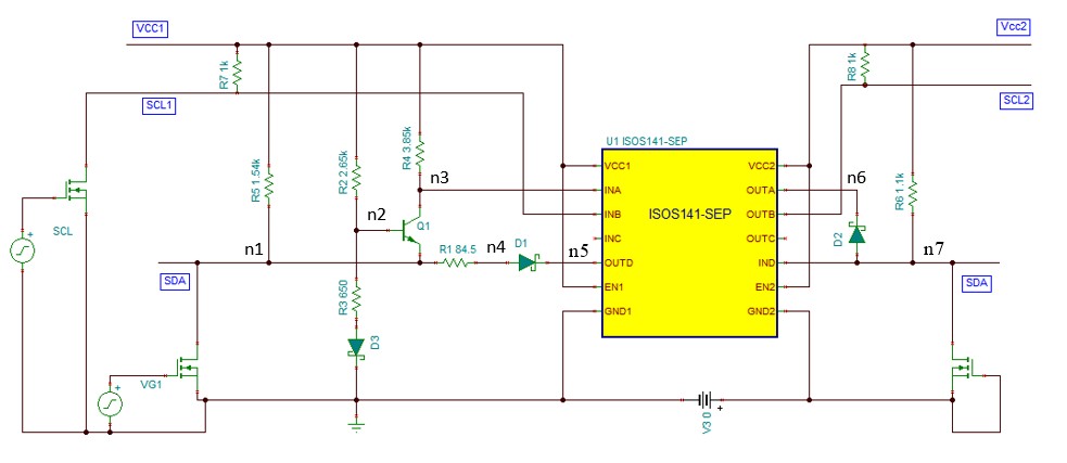
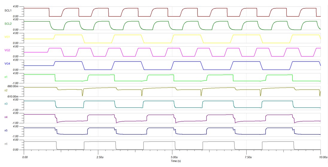
The following figure shows the final isolated I2C circuit whether the primary is isolated from a secondary bus. Only the SDA data line is bidirectional, and the SCL clock line is unidirectional. A pulse generator with 500kHz is set at the primary SDA to simulate the 1Mbps 0101 data pattern transmitted from n1 to n7. As shown in the lower figure, n1 is pulled down to logic low. This causes n3 to go to logic low and pass the value from the input INA to output OUTA. Hence n6 and n7 are pulled down to logic low. When SDA is released, n1 voltage only returns to logic high after the n7 voltage goes to logic high.
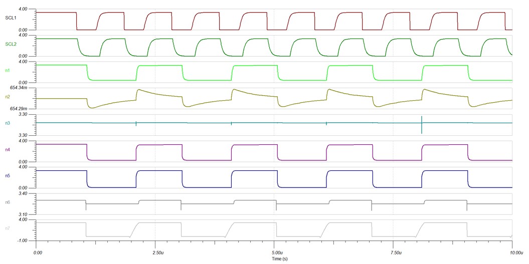
A pulse generator with 500kHz is set at the secondary SDA to simulate the 1Mbps 0101 data pattern transmitted from n7 to n1. As shown in the lower figure, n7 is pulled down to logic low and passing the value from the input IND to output OUTD. Hence n5 and n4 are pulled down to logic low. The n1 voltage is 0.17V higher than the n4 voltage due to the voltage drop across R1 but still well below VILmax.
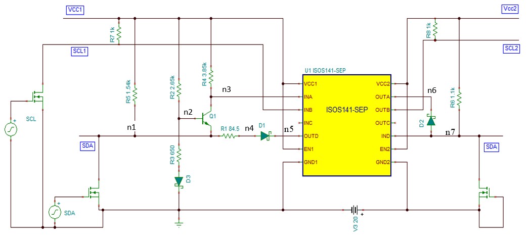
A pulse generator with 500kHz is set at the primary SDA to simulate the 1Mbps 0101 data pattern transmitted from n1 to n7. The secondary side ground is raised by 20 V to simulate the performance of the isolated I2C. As shown in the following image, The primary side SDA (n1) operates from 0 V to 3.3 V, and the secondary side SCL and SDA (n7) operate from 20 V to 23.3 V due to ground bounds.
Reference
| ISOS141-SEP | |
|---|---|
| VCC1, Vcc2 | 2.25 V to 5.5 V |
| Data-rate | 100MHz |
| Propagation delay | 10.7ns to 16ns |
| TID Characterized (ELDRS-Free) | 30krad(Si) |
| TID RLAT, RHA | 30krad(Si) |
| CMTI | ±100kV/µs |
| VISO | 3000 VRMS |
| www.ti.com/product/ISOS141-SEP | |