SNLS493A October 2014 – January 2015 DS80PCI810
PRODUCTION DATA.
- 1 Features
- 2 Applications
- 3 Description
- 4 Revision History
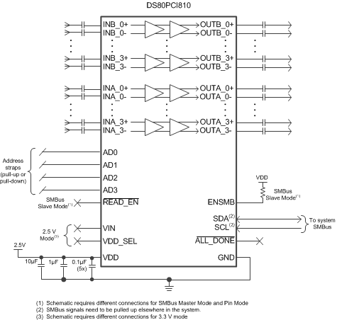
- 5 Pin Configuration and Functions
- 6 Specifications
- 7 Detailed Description
- 8 Applications and Implementation
- 9 Power Supply Recommendations
- 10Layout
- 11Device and Documentation Support
- 12Mechanical, Packaging, and Orderable Information
1 Features
- Low 70 mW/Channel (Typ) Power Consumption, With Option to Power Down Unused Channels
- Seamless Link Training Support
- Advanced Configurable Signal Conditioning I/O
- Receive CTLE up to ~10 dB at 4 GHz
- Linear Output Driver
- Variable Output Voltage Range up to 1200 mVp-p
- Automatic Receiver Detect (Hot-Plug)
- Ultra-Low Input-to-Output Latency: 80 ps (Typ)
- Programmable via Pin Selection, EEPROM, or SMBus Interface
- Single Supply Voltage: 2.5 V or 3.3 V
- 4 kV HBM ESD Rating
- −40°C to 85°C Operating Temperature Range
- Flow-Thru Layout in 10 mm x 5.5 mm 54-Pin Leadless WQFN Package
- Pin Compatible with DS80PCI800
2 Applications
- PCI Express Gen-1, 2, and 3
- Other Proprietary High Speed Interfaces Up to 8 Gbps
Simplified Functional Block Diagram
3 Description
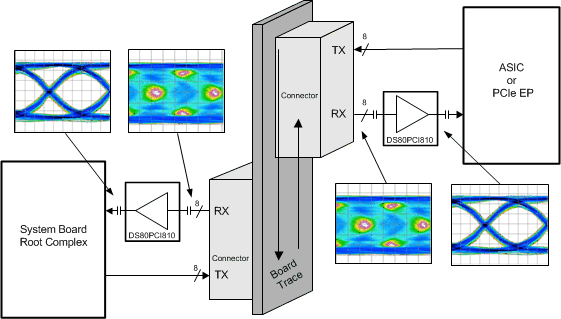
The DS80PCI810 is an extremely low-power high-performance repeater/redriver designed to support eight channels carrying high speed interface up to 8 Gbps, such as PCIe Gen-1, 2, and 3. The receiver's continuous time linear equalizer (CTLE) provides high frequency boost that is programmable from 2.7 to 9.5 dB at 4 GHz (8 Gbps) followed by a linear output driver. The CTLE receiver is capable of opening an input eye that is completely closed due to inter symbol interference (ISI) induced by interconnect medium such as board traces or twin axial-copper cables. The programmable equalization maximizes the flexibility of physical placement within the interconnect channel and improves overall channel performance.
When operating in PCIe applications, the DS80PCI810 preserves transmit signal characteristics, thereby allowing the host controller and the end point to negotiate transmit equalizer coefficients. This transparency in the link training protocol facilitates system level interoperability and minimizes latency.
The programmable settings can be applied easily via pin control, software (SMBus or I2C), or direct loading from an external EEPROM. In EEPROM mode, the configuration information is automatically loaded on power up, thereby eliminating the need for an external microprocessor or software driver.
Device Information(1)
| PART NUMBER | PACKAGE | BODY SIZE (NOM) |
|---|---|---|
| DS80PCI810 | WQFN (54) | 10 mm x 5.5 mm |
- For all available packages, see the orderable addendum at the end of the datasheet.
Typical Application Block Diagram