SLUSBD0E June 2013 – December 2014 UCC27527 , UCC27528
PRODUCTION DATA.
- 1 Features
- 2 Applications
- 3 Description
- 4 Revision History
- 5 Description (continued)
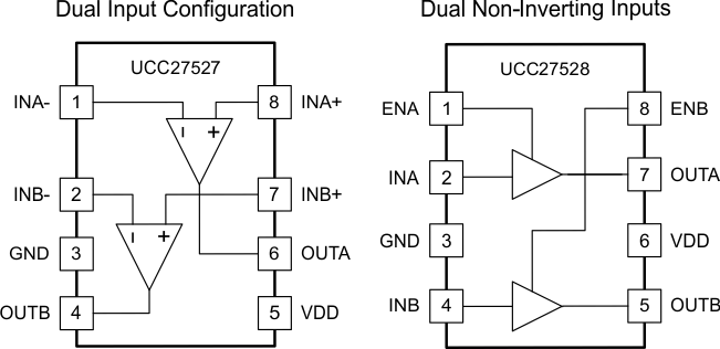
- 6 Pin Configuration and Functions
- 7 Specifications
- 8 Detailed Description
- 9 Application and Implementation
- 10Power Supply Recommendations
- 11Layout
- 12Device and Documentation Support
- 13Mechanical, Packaging, and Orderable Information
パッケージ・オプション
メカニカル・データ(パッケージ|ピン)
サーマルパッド・メカニカル・データ
発注情報
1 Features
- Industry-Standard Pin Out
- Two Independent Gate-Drive Channels
- 5-A Peak Source and Sink Drive Current
- CMOS Input Logic Threshold
(Function of Supply Voltage on VDD Pins) - Hysteretic Logic Thresholds for High Noise Immunity
- Independent Enable Function for Each Output
- Inputs and Enable Pin Voltage Levels Not Restricted by VDD Pin Bias Supply Voltage
- 4.5-V to 18-V Single Supply Range
- Outputs Held Low During VDD UVLO (Ensures Glitch-Free Operation at Power Up and Power Down)
- Fast Propagation Delays (17-ns Typical)
- Fast Rise and Fall Times (7-ns and 6-ns Typical)
- 1-ns Typical Delay Matching Between 2 Channels
- Outputs Held in Low When Inputs Floating
- SOIC-8, and 3-mm x 3-mm WSON-8 Package Options
- Operating Temperature Range of –40°C to 140°C
- –5-V Negative Voltage Handling Capability on Input Pins
2 Applications
- Switch-Mode Power Supplies
- DC-to-DC Converters
- Motor Control, Solar Power
- Gate Drive for Emerging Wideband Gap Power Devices Such as GaN
3 Description
The UCC2752x family of devices are dual-channel, high-speed, low-side gate driver devices capable of effectively driving MOSFET and IGBT power switches. Using a design that inherently minimizes shoot-through current, UCC2752x can deliver high-peak current pulses of up to 5-A source and 5-A sink into capacitive loads along with rail-to-rail drive capability and extremely small propagation delay typically 17 ns. In addition, the drivers feature matched internal propagation delays between the two channels which are very well suited for applications requiring dual-gate drives with critical timing, such as synchronous rectifiers. The input pin thresholds are based on CMOS logic, which is a function of the VDD supply voltage. Wide hysteresis between the high and low thresholds offers excellent noise immunity. The Enable pins are based on TTL and CMOS compatible logic, independent of VDD supply voltage.
Device Information(1)
| PART NUMBER | PACKAGE | BODY SIZE (NOM) |
|---|---|---|
| UCC27527 | WSON (8) | 3.00 mm x 3.00 mm |
| SOIC (8) | 4.90 mm x 3.91 mm | |
| UCC27528 | WSON (8) | 3.00 mm x 3.00 mm |
| SOIC (8) | 4.90 mm x 3.91 mm |
- For all available packages, see the orderable addendum at the end of the datasheet.