SNOSD59 June 2017
PRODUCTION DATA.
- 1 Features
- 2 Applications
- 3 Description
- 4 Revision History
- 5 Pin Configuration and Functions
- 6 Specifications
- 7 Detailed Description
- 8 Application and Implementation
- 9 Power Supply Recommendations
- 10Layout
- 11Device and Documentation Support
- 12Mechanical, Packaging, and Orderable Information
Package Options
Mechanical Data (Package|Pins)
- YS|0
- LMC|8
Thermal pad, mechanical data (Package|Pins)
Orderable Information
1 Features
- 1/10 Supply Current of a LM1458: 400 μA (Max)
- Low Input Bias Current: 50 pA (Max)
- Low Input Offset Voltage: 1 mV (Max)
- Low Input Offset Voltage Drift: 7 μV/°C (Typ)
- High Gain Bandwidth: 1 MHz
- High Slew Rate: 1 V/μs
- Low Noise Voltage for Low Power: 35 nV/√Hz
- Low Input Noise Current: 0.01 pA/√Hz
- High Input Impedance: 1012Ω
- High Gain VO = ±10V, RL = 10k: 50k (Min)
2 Applications
- High Speed Integrators
- Fast D/A Converters
- Sample and Hold Circuits
3 Description
The LF442-MIL dual low power operational amplifiers provide many of the same AC characteristics as the industry standard LM1458 while greatly improving the DC characteristics of the LM1458. The amplifiers have the same bandwidth, slew rate, and gain (10 kΩ load) as the LM1458 and only draw one tenth the supply current of the LM1458. In addition the well matched high voltage JFET input devices of the LF442-MIL reduce the input bias and offset currents by a factor of 10,000 over the LM1458. A combination of careful layout design and internal trimming ensures very low input offset voltage and voltage drift. The LF442-MIL also has a very low equivalent input noise voltage for a low power amplifier.
The LF442-MIL is pin compatible with the LM1458 allowing an immediate 10 times reduction in power drain in many applications. The LF442-MIL should be used where low power dissipation and good electrical characteristics are the major considerations.
Device Information(1)
| PART NUMBER | PACKAGE | BODY SIZE (NOM) |
|---|---|---|
| LF442-MILACN | PDIP (8) | 9.59 mm × 6.35 mm |
| LF442-MILAMH | TO-99 (8) | 8.96 mm Diameter |
- For all available packages, see the orderable addendum at the end of the data sheet.
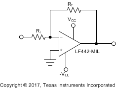
Inverting Amplifier

4 Revision History
| DATE | REVISION | NOTES |
|---|---|---|
| June 2017 | * | Initial release. |