SBAA515A June 2021 – September 2022 AMC3301 , AMC3301-Q1 , AMC3302 , AMC3302-Q1 , AMC3306M05 , AMC3306M25 , AMC3330 , AMC3330-Q1 , AMC3336 , AMC3336-Q1
4.2 PCB Layout Best Practices for Multiple AMC3301
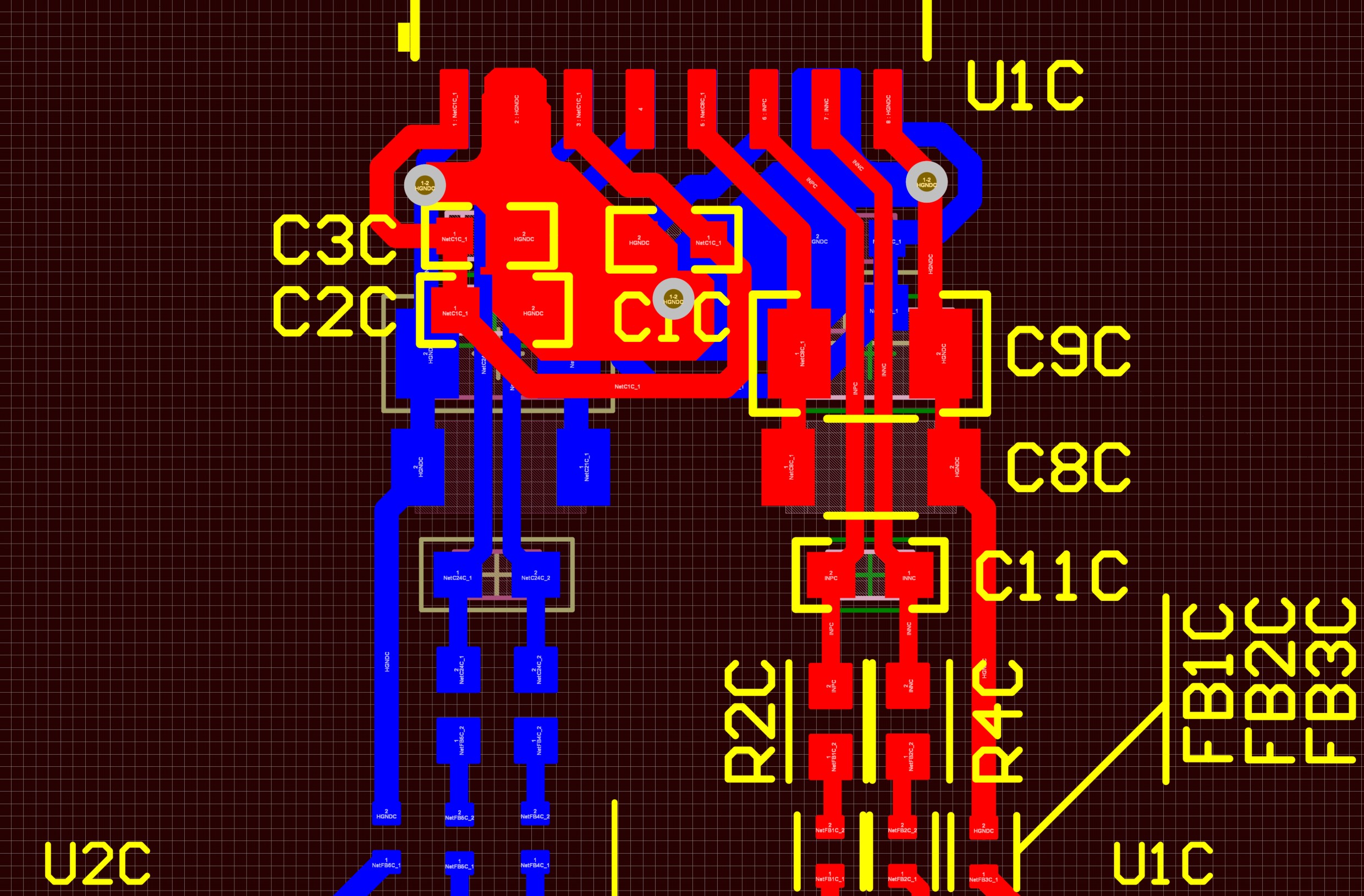
The schematic used in testing is the same as the ferrite section of Figure 4-3. However, layout for stacking the AMC3301’s is shown in Figure 4-3.
 Figure 4-3 Recommended Multiple AMC3301
Devices Layout
Figure 4-3 Recommended Multiple AMC3301
Devices LayoutIn general, the same layout principles described in Section 3.2 are followed with a two layer board design.
However, a direct and low inductance path from pin 2 (DCDC_HGND) to pin 8 (HGND) of each device is achieved differently. Instead of a trace, a star connection connects both devices between the top and bottom layers at pins 4 and 5. In addition, a pool of copper is used to connect the DC/DC capacitors to DCDC_HGND on the same layer.
Finally, the LDO_OUT capacitors are scaled up to a 1206 package to allow direct and uninterrupted path for the positive and negative inputs underneath the capacitors.