SBAS502C December 2011 – April 2020 ADS1291 , ADS1292 , ADS1292R
PRODUCTION DATA.
- 1 Features
- 2 Applications
- 3 Description
- 4 Revision History
- 5 Pin Configuration and Functions
- 6 Specifications
- 7 Parameter Measurement Information
-
8 Detailed Description
- 8.1 Overview
- 8.2 Functional Block Diagram
- 8.3
Feature Description
- 8.3.1 EMI Filter
- 8.3.2
Input Multiplexer
- 8.3.2.1 Device Noise Measurements
- 8.3.2.2 Test Signals (TestP and TestN)
- 8.3.2.3 Auxiliary Differential Input (RESP_MODN/IN3N, RESP_MODN/IN3P)
- 8.3.2.4 Temperature Sensor (TEMPP, TEMPN)
- 8.3.2.5 Supply Measurements (MVDDP, MVDDN)
- 8.3.2.6 Lead-Off Excitation Signals (LoffP, LoffN)
- 8.3.2.7 Auxiliary Single-Ended Input
- 8.3.3 Analog Input
- 8.3.4 PGA Settings and Input Range
- 8.3.5 Digital Decimation Filter
- 8.3.6 Reference
- 8.3.7 Clock
- 8.3.8 Data Format
- 8.3.9 Multiple Device Configuration
- 8.3.10 ECG-Specific Functions
- 8.3.11 Setting the Device for Basic Data Capture
- 8.4 Device Functional Modes
- 8.5
Programming
- 8.5.1 SPI Interface
- 8.5.2
SPI Command Definitions
- 8.5.2.1 WAKEUP: Exit STANDBY Mode
- 8.5.2.2 STANDBY: Enter STANDBY Mode
- 8.5.2.3 RESET: Reset Registers to Default Values
- 8.5.2.4 START: Start Conversions
- 8.5.2.5 STOP: Stop Conversions
- 8.5.2.6 OFFSETCAL: Channel Offset Calibration
- 8.5.2.7 RDATAC: Read Data Continuous
- 8.5.2.8 SDATAC: Stop Read Data Continuous
- 8.5.2.9 RDATA: Read Data
- 8.5.2.10 Sending Multi-Byte Commands
- 8.5.2.11 RREG: Read From Register
- 8.5.2.12 WREG: Write to Register
- 8.6
Register Maps
- 8.6.1
User Register Description
- 8.6.1.1 ID: ID Control Register (Factory-Programmed, Read-Only) (address = 00h)
- 8.6.1.2 CONFIG1: Configuration Register 1 (address = 01h)
- 8.6.1.3 CONFIG2: Configuration Register 2 (address = 02h)
- 8.6.1.4 LOFF: Lead-Off Control Register (address = 03h)
- 8.6.1.5 CH1SET: Channel 1 Settings (address = 04h)
- 8.6.1.6 CH2SET: Channel 2 Settings (address = 05h)
- 8.6.1.7 RLD_SENS: Right Leg Drive Sense Selection (address = 06h)
- 8.6.1.8 LOFF_SENS: Lead-Off Sense Selection (address = 07h)
- 8.6.1.9 LOFF_STAT: Lead-Off Status (address = 08h)
- 8.6.1.10 RESP1: Respiration Control Register 1 (address = 09h)
- 8.6.1.11 RESP2: Respiration Control Register 2 (address = 0Ah)
- 8.6.1.12 GPIO: General-Purpose I/O Register (address = 0Bh)
- 8.6.1
User Register Description
- 9 Application and Implementation
- 10Power Supply Recommendations
- 11Layout
- 12Device and Documentation Support
- 13Mechanical, Packaging, and Orderable Information
8.3.4 PGA Settings and Input Range
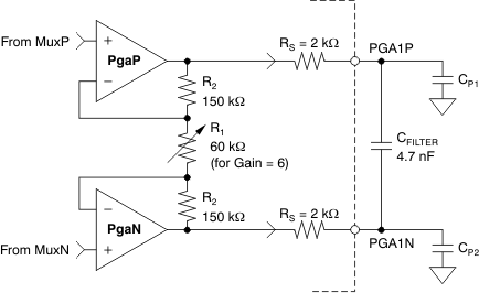
The PGA is a differential input or differential output amplifier, as shown in Figure 22. It has seven gain settings (1, 2, 3, 4, 6, 8, and 12) that can be set by writing to the CHnSET register (see the CH1SET and CH2SET Registers in the Register Map section for details). The ADS1291, ADS1292, and ADS1292R have CMOS inputs and hence have negligible current noise.
 Figure 22. PGA Implementation
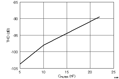
 The PGA resistor string that implements the gain has 360 kΩ of resistance for a gain of 6. This resistance provides a current path across the outputs of the PGA in the presence of a differential input signal. This current is in addition to the quiescent current specified for the device in the presence of a differential signal at the input. The PGA output is filtered by an RC filter before it goes to the ADC. The filter is formed by an internal resistor RS = 2 kΩ and an external capacitor CFILTER (4.7 nF, typical). This filter acts as an anti-aliasing filter with the –3-dB bandwidth of 8.4 kHz. The internal RS resistor is accurate to 15% so actual bandwidth will vary. This RC filter also suppresses the glitch at the PGA output caused by ADC sampling. The minimum value of CEXT that can be used is 4 nF. A larger value CFILTER capacitor can be used for increased attenuation at higher frequencies for anti-aliasing purposes. If channel 1 of the ADS1292R is used for respiration measurement, then a 4.7-nF external capacitor is recommended. The tradeoff is that a larger capacitor value gives degraded THD performance. See Figure 23 for a diagram explaining the THD versus CFILTER value for a 10-Hz input signal.
 Figure 23. THD versus CFILTER Value
 Special care must be taken in PCB layout to minimize the parasitic capacitance CP1 / CP2. The absolute value of these capacitances must be less than 20 pF. Ideally, CFILTER should be placed right at the pins to minimize these capacitors. Mismatch between these capacitors will lead to CMRR degradation. Assuming everything else is perfectly matched, the 60-Hz CMRR as a function of this mismatch is given by Equation 4.

where ΔCP = CP1 – CP2
For example, a mismatch of 20 pF with a gain of 6 limits the CMRR to 112 dB. If ΔCP is small, then the CMRR is limited by the PGA itself and is as specified in the Electrical Characteristics table. The PGA are chopped internally at either 8, 32, or 64 kSPS, as determined by the CHOP bits (see the RLD_SENS: Right Leg Drive Sense Selection register, bits[7:6]). The digital decimation filter filters out the chopping ripple in the normal path so the chopping ripple is not a concern. If PGA output is used for hardware PACE detection, the chopping ripple must be filtered. First-order filtering is provided by the RC filter at the PGA output. Additional filtering may be needed to suppress the chopping ripple. If the PGA output is routed to other circuitry, a 20-kΩ series resistance must be added in the path near the CFILTER capacitor. The routing should be matched to maintain the CMRR performance.