SBAS550C June 2011 – May 2015 ADS4229
PRODUCTION DATA.
- 1 Features
- 2 Applications
- 3 Description
- 4 Revision History
- 5 Device Comparison Table
- 6 Pin Configuration and Functions
-
7 Specifications
- 7.1 Absolute Maximum Ratings
- 7.2 ESD Ratings
- 7.3 Recommended Operating Conditions
- 7.4 Thermal Information
- 7.5 Electrical Characteristics: ADS4229 (250 MSPS)
- 7.6 Electrical Characteristics: General
- 7.7 Digital Characteristics
- 7.8 LVDS and CMOS Modes Timing Requirements
- 7.9 LVDS Timings at Lower Sampling Frequencies
- 7.10 CMOS Timings at Lower Sampling Frequencies
- 7.11 Serial Interface Timing Characteristics
- 7.12 Reset Timing (Only when Serial Interface is Used)
- 7.13 Typical Characteristics
-
8 Detailed Description
- 8.1 Overview
- 8.2 Functional Block Diagram
- 8.3 Feature Description
- 8.4 Device Functional Modes
- 8.5 Programming
- 8.6
Register Maps
- 8.6.1 Serial Register Map
- 8.6.2
Description of Serial Registers
- 8.6.2.1 Register Address 00h (Default = 00h)
- 8.6.2.2 Register Address 01h (Default = 00h)
- 8.6.2.3 Register Address 03h (Default = 00h)
- 8.6.2.4 Register Address 25h (Default = 00h)
- 8.6.2.5 Register Address 29h (Default = 00h)
- 8.6.2.6 Register Address 2Bh (Default = 00h)
- 8.6.2.7 Register Address 3Dh (Default = 00h)
- 8.6.2.8 Register Address 3Fh (Default = 00h)
- 8.6.2.9 Register Address 40h (Default = 00h)
- 8.6.2.10 Register Address 41h (Default = 00h)
- 8.6.2.11 Register Address 42h (Default = 00h)
- 8.6.2.12 Register Address 45h (Default = 00h)
- 8.6.2.13 Register Address 4Ah (Default = 00h)
- 8.6.2.14 Register Address 58h (Default = 00h)
- 8.6.2.15 Register Address BFh (Default = 00h)
- 8.6.2.16 Register Address C1h (Default = 00h)
- 8.6.2.17 Register Address CFh (Default = 00h)
- 8.6.2.18 Register Address EFh (Default = 00h)
- 8.6.2.19 Register Address F1h (Default = 00h)
- 8.6.2.20 Register Address F2h (Default = 00h)
- 8.6.2.21 Register Address 2h (Default = 00h)
- 8.6.2.22 Register Address D5h (Default = 00h)
- 8.6.2.23 Register Address D7h (Default = 00h)
- 8.6.2.24 Register Address DBh (Default = 00h)
- 9 Application and Implementation
- 10Power Supply Recommendations
- 11Layout
- 12Device and Documentation Support
- 13Mechanical, Packaging, and Orderable Information
7 Specifications
7.1 Absolute Maximum Ratings(1)
| MIN | MAX | UNIT | ||
|---|---|---|---|---|
| Supply voltage, AVDD | –0.3 | 2.1 | V | |
| Supply voltage, DRVDD | –0.3 | 2.1 | V | |
| Voltage between AGND and DRGND | –0.3 | 0.3 | V | |
| Voltage between AVDD to DRVDD (when AVDD leads DRVDD) | –2.4 | 2.4 | V | |
| Voltage between DRVDD to AVDD (when DRVDD leads AVDD) | –2.4 | 2.4 | V | |
| Voltage applied to input pins | INP_A, INM_A, INP_B, INM_B | –0.3 | Minimum (1.9, AVDD + 0.3) |
V |
| CLKP, CLKM(2) | –0.3 | AVDD + 0.3 | V | |
| RESET, SCLK, SDATA, SEN, CTRL1, CTRL2, CTRL3 |
–0.3 | 3.9 | V | |
| Operating free-air temperature, TA | –40 | 85 | °C | |
| Operating junction temperature, TJ | 125 | °C | ||
| Storage temperature, Tstg | –65 | 150 | °C | |
(1) Stresses beyond those listed under Absolute Maximum Ratings may cause permanent damage to the device. These are stress ratings only, which do not imply functional operation of the device at these or any other conditions beyond those indicated under Recommended Operating Conditions. Exposure to absolute-maximum-rated conditions for extended periods may affect device reliability.
(2) When AVDD is turned off, it is recommended to switch off the input clock (or ensure the voltage on CLKP, CLKM is less than |0.3 V|). This configuration prevents the ESD protection diodes at the clock input pins from turning on.
7.2 ESD Ratings
| VALUE | UNIT | |||
|---|---|---|---|---|
| V(ESD) | Electrostatic discharge | Human body model (HBM), per ANSI/ESDA/JEDEC JS-001(1) | 2000 | V |
(1) JEDEC document JEP155 states that 500-V HBM allows safe manufacturing with a standard ESD control process.
7.3 Recommended Operating Conditions
Over operating free-air temperature range, unless otherwise noted.| MIN | NOM | MAX | UNIT | ||
|---|---|---|---|---|---|
| SUPPLIES | |||||
| Analog supply voltage, AVDD | 1.7 | 1.8 | 1.9 | V | |
| Digital supply voltage, DRVDD | 1.7 | 1.8 | 1.9 | V | |
| ANALOG INPUTS | |||||
| Differential input voltage range | 2 | VPP | |||
| Input common-mode voltage | VCM ± 0.05 | V | |||
| Maximum analog input frequency with 2-VPP input amplitude(1) | 400 | MHz | |||
| Maximum analog input frequency with 1-VPP input amplitude(1) | 600 | MHz | |||
| CLOCK INPUT | |||||
| Input clock sample rate | |||||
| Low-speed mode enabled(2) | 1 | 80 | MSPS | ||
| Low-speed mode disabled(2) (by default after reset) | 80 | 250 | MSPS | ||
| Input clock amplitude differential (VCLKP – VCLKM) |
Sine wave, ac-coupled | 0.2 | 1.5 | VPP | |
| LVPECL, ac-coupled | 1.6 | VPP | |||
| LVDS, ac-coupled | 0.7 | VPP | |||
| LVCMOS, single-ended, ac-coupled | 1.5 | V | |||
| Input clock duty cycle | |||||
| Low-speed mode disabled | 35% | 50% | 65% | ||
| Low-speed mode enabled | 40% | 50% | 60% | ||
| DIGITAL OUTPUTS | |||||
| Maximum external load capacitance from each output pin to DRGND, CLOAD | 5 | pF | |||
| Differential load resistance between the LVDS output pairs (LVDS mode), RLOAD | 100 | Ω | |||
| Operating free-air temperature, TA | –40 | +85 | °C | ||
(1) See Theory of Operation
(2) See Serial Interface Configuration for details on programming the low-speed mode.
7.4 Thermal Information
| THERMAL METRIC(1) | ADS4229 | UNIT | |
|---|---|---|---|
| RGC (VQFN) | |||
| 64 PINS | |||
| RθJA | Junction-to-ambient thermal resistance | 23.9 | °C/W |
| RθJC(top) | Junction-to-case (top) thermal resistance | 10.9 | °C/W |
| RθJB | Junction-to-board thermal resistance | 4.3 | °C/W |
| ψJT | Junction-to-top characterization parameter | 0.1 | °C/W |
| ψJB | Junction-to-board characterization parameter | 4.4 | °C/W |
| RθJC(bot) | Junction-to-case (bottom) thermal resistance | 0.6 | °C/W |
(1) For more information about traditional and new thermal metrics, see the Semiconductor and IC Package Thermal Metrics application report, SPRA953.
7.5 Electrical Characteristics: ADS4229 (250 MSPS)
Typical values are at +25°C, AVDD = 1.8 V, DRVDD = 1.8 V, 50% clock duty cycle, –1 dBFS differential analog input, LVDS interface, and 0-dB gain, unless otherwise noted. Minimum and maximum values are across the full temperature range:TMIN = –40°C to TMAX = +85°C, AVDD = 1.8 V, and DRVDD = 1.8 V.
7.6 Electrical Characteristics: General
Typical values are at +25°C, AVDD = 1.8 V, DRVDD = 1.8 V, 50% clock duty cycle, and –1 dBFS differential analog input, unless otherwise noted. Minimum and maximum values are across the full temperature range: TMIN = –40°C to TMAX = +85°C, AVDD = 1.8 V, and DRVDD = 1.8 V.| PARAMETER | MIN | TYP | MAX | UNIT | |
|---|---|---|---|---|---|
| ANALOG INPUTS | |||||
| Differential input voltage range | 2 | VPP | |||
| Differential input resistance (at 200 MHz) | 0.75 | kΩ | |||
| Differential input capacitance (at 200 MHz) | 3.7 | pF | |||
| Analog input bandwidth (with 50-Ω source impedance, and 50-Ω termination) |
550 | MHz | |||
| Analog input common-mode current (per input pin of each channel) |
1.5 | µA/MSPS | |||
| Common-mode output voltage | VCM | 0.95(2) | V | ||
| VCM output current capability | 4 | mA | |||
| DC ACCURACY | |||||
| Offset error | –15 | 2.5 | 15 | mV | |
| Temperature coefficient of offset error | 0.003 | mV/°C | |||
| Gain error as a result of internal reference inaccuracy alone | EGREF | –2 | 2 | %FS | |
| Gain error of channel alone | EGCHAN | ±0.1 | 1 | %FS | |
| Temperature coefficient of EGCHAN | 0.002 | Δ%/°C | |||
| POWER SUPPLY | |||||
| IAVDD Analog supply current |
167 | 190 | mA | ||
| IDRVDD Output buffer supply current LVDS interface, 350-mV swing with 100-Ω external termination, fIN = 2.5 MHz |
136 | 160 | mA | ||
| IDRVDD Output buffer supply current CMOS interface, no load capacitance, fIN = 2.5 MHz(1) |
94 | mA | |||
| Analog power | 301 | mW | |||
| Digital power LVDS interface, 350-mV swing with 100-Ω external termination, fIN = 2.5 MHz |
245 | mW | |||
| Digital power CMOS interface, 8-pF external load capacitance(1) fIN = 2.5 MHz |
169 | mW | |||
| Global power-down | 25 | mW | |||
(1) In CMOS mode, the DRVDD current scales with the sampling frequency, the load capacitance on output pins, input frequency, and the supply voltage (see CMOS Interface Power Dissipation).
(2) VCM changes to 0.87 V when the HIGH PERF MODE[7:2] serial register bits are set.
7.7 Digital Characteristics
At AVDD = 1.8 V and DRVDD = 1.8 V, unless otherwise noted. DC specifications refer to the condition where the digital outputs do not switch, but are permanently at a valid logic level '0' or '1'.| PARAMETER | TEST CONDITIONS | MIN | TYP | MAX | UNIT | |
|---|---|---|---|---|---|---|
| DIGITAL INPUTS (RESET, SCLK, SDATA, SEN, CTRL1, CTRL2, CTRL3)(1) | ||||||
| High-level input voltage | All digital inputs support 1.8-V and 3.3-V CMOS logic levels | 1.3 | V | |||
| Low-level input voltage | 0.4 | V | ||||
| High-level input current | SDATA, SCLK(2) | VHIGH = 1.8 V | 10 | µA | ||
| SEN(3) | VHIGH = 1.8 V | 0 | µA | |||
| Low-level input current | SDATA, SCLK | VLOW = 0 V | 0 | µA | ||
| SEN | VLOW = 0 V | 10 | µA | |||
| DIGITAL OUTPUTS, CMOS INTERFACE (DA[13:0], DB[13:0], CLKOUT, SDOUT) | ||||||
| High-level output voltage | DRVDD – 0.1 | DRVDD | V | |||
| Low-level output voltage | 0 | 0.1 | V | |||
| Output capacitance (internal to device) | pF | |||||
| DIGITAL OUTPUTS, LVDS INTERFACE | ||||||
| High-level output differential voltage |
VODH | With an external 100-Ω termination |
270 | 350 | 430 | mV |
| Low-level output differential voltage |
VODL | With an external 100-Ω termination |
–430 | –350 | –270 | mV |
| Output common-mode voltage | VOCM | 0.9 | 1.05 | 1.25 | V | |
(1) SCLK, SDATA, and SEN function as digital input pins in serial configuration mode.
(2) SDATA, SCLK have internal 150-kΩ pull-down resistor.
(3) SEN has an internal 150-kΩ pull-up resistor to AVDD. Because the pull-up is weak, SEN can also be driven by 1.8 V or 3.3 V CMOS buffers.

1. With external 100-Ω termination.
Figure 1. LVDS Output Voltage Levels
7.8 LVDS and CMOS Modes Timing Requirements(1)
Typical values are at +25°C, AVDD = 1.8 V, DRVDD = 1.8 V, sampling frequency = 250 MSPS, sine wave input clock, CLOAD = 5 pF, and RLOAD = 100 Ω, unless otherwise noted. Minimum and maximum values are across the full temperature range: TMIN = –40°C to TMAX = +85°C, AVDD = 1.8 V, and DRVDD = 1.7 V to 1.9 V.| PARAMETER | DESCRIPTION | MIN | TYP | MAX | UNIT | |
|---|---|---|---|---|---|---|
| tA | Aperture delay | 0.5 | 0.8 | 1.1 | ns | |
| Aperture delay matching | Between the two channels of the same device | ±70 | ps | |||
| Variation of aperture delay | Between two devices at the same temperature and DRVDD supply | ±150 | ps | |||
| tJ | Aperture jitter | 140 | fS rms | |||
| Wakeup time | Time to valid data after coming out of STANDBY mode | 50 | 100 | µs | ||
| Time to valid data after coming out of GLOBAL power-down mode | 100 | 500 | µs | |||
| ADC latency(4) | Default latency after reset | 16 | Clock cycles | |||
| Digital functions enabled (EN DIGITAL = 1) | 24 | Clock cycles | ||||
| DDR LVDS MODE(2) | ||||||
| tSU | Data setup time | Data valid(3) to zero-crossing of CLKOUTP | 0.6 | 0.88 | ns | |
| tH | Data hold time | Zero-crossing of CLKOUTP to data becoming invalid(3) | 0.33 | 0.55 | ns | |
| tPDI | Clock propagation delay | Input clock rising edge cross-over to output clock rising edge cross-over | 5 | 6 | 7.5 | ns |
| LVDS bit clock duty cycle | Duty cycle of differential clock, (CLKOUTP-CLKOUTM) | 48% | ||||
| tRISE, tFALL |
Data rise time, Data fall time |
Rise time measured from –100 mV to +100 mV Fall time measured from +100 mV to –100 mV 1 MSPS ≤ Sampling frequency ≤ 250 MSPS |
0.13 | ns | ||
| tCLKRISE, tCLKFALL |
Output clock rise time, Output clock fall time |
Rise time measured from –100 mV to +100 mV Fall time measured from +100 mV to –100 mV 1 MSPS ≤ Sampling frequency ≤ 250 MSPS |
0.13 | ns | ||
| PARALLEL CMOS MODE | ||||||
| tPDI | Clock propagation delay | Input clock rising edge cross-over to output clock rising edge cross-over | 4.5 | 6.2 | 8.5 | ns |
| Output clock duty cycle | Duty cycle of output clock, CLKOUT 1 MSPS ≤ Sampling frequency ≤ 200 MSPS |
50% | ||||
| tRISE, tFALL |
Data rise time, Data fall time |
Rise time measured from 20% to 80% of DRVDD Fall time measured from 80% to 20% of DRVDD 1 MSPS ≤ Sampling frequency ≤ 200 MSPS |
0.7 | ns | ||
| tCLKRISE, tCLKFALL |
Output clock rise time Output clock fall time |
Rise time measured from 20% to 80% of DRVDD Fall time measured from 80% to 20% of DRVDD 1 MSPS ≤ Sampling frequency ≤ 200 MSPS |
0.7 | ns | ||
(1) Timing parameters are ensured by design and characterization and not tested in production.
(2) Measurements are done with a transmission line of 100-Ω characteristic impedance between the device and the load. Setup and hold time specifications take into account the effect of jitter on the output data and clock.
(3) Data valid refers to a logic high of +100 mV and a logic low of –100 mV.
(4) At higher frequencies, tPDI is greater than one clock period and overall latency = ADC latency + 1.
7.9 LVDS Timings at Lower Sampling Frequencies
Typical values are at +25°C, AVDD = 1.8 V, DRVDD = 1.8 V, sampling frequency = 250 MSPS, sine wave input clock, CLOAD = 5 pF, and RLOAD = 100 Ω, unless otherwise noted. Minimum and maximum values are across the full temperature range: TMIN = –40°C to TMAX = +85°C, AVDD = 1.8 V, and DRVDD = 1.7 V to 1.9 V.| SAMPLING FREQUENCY (MSPS) | SETUP TIME (ns) | HOLD TIME (ns) | tPDI, CLOCK PROPAGATION DELAY (ns) |
||||||
|---|---|---|---|---|---|---|---|---|---|
| MIN | TYP | MAX | MIN | TYP | MAX | MIN | TYP | MAX | |
| 65 | 5.9 | 6.6 | 0.35 | 0.6 | 5 | 6 | 7.5 | ||
| 80 | 4.5 | 5.2 | 0.35 | 0.6 | 5 | 6 | 7.5 | ||
| 125 | 2.3 | 2.9 | 0.35 | 0.6 | 5 | 6 | 7.5 | ||
| 160 | 1.5 | 2 | 0.33 | 0.55 | 5 | 6 | 7.5 | ||
| 185 | 1.3 | 1.6 | 0.33 | 0.55 | 5 | 6 | 7.5 | ||
| 200 | 1.1 | 1.4 | 0.33 | 0.55 | 5 | 6 | 7.5 | ||
| 230 | 0.76 | 1.06 | 0.33 | 0.55 | 5 | 6 | 7.5 | ||
7.10 CMOS Timings at Lower Sampling Frequencies
Typical values are at +25°C, AVDD = 1.8 V, DRVDD = 1.8 V, sampling frequency = 250 MSPS, sine wave input clock, CLOAD = 5 pF, and RLOAD = 100 Ω, unless otherwise noted. Minimum and maximum values are across the full temperature range: TMIN = –40°C to TMAX = +85°C, AVDD = 1.8 V, and DRVDD = 1.7 V to 1.9 V.| SAMPLING FREQUENCY (MSPS) | TIMINGS SPECIFIED WITH RESPECT TO CLKOUT | ||||||||
|---|---|---|---|---|---|---|---|---|---|
| SETUP TIME(1) (ns) | HOLD TIME(1) (ns) | tPDI, CLOCK PROPAGATION DELAY (ns) |
|||||||
| MIN | TYP | MAX | MIN | TYP | MAX | MIN | TYP | MAX | |
| 65 | 6.1 | 6.7 | 6.7 | 7.5 | 4.5 | 6.2 | 8.5 | ||
| 80 | 4.7 | 5.2 | 5.3 | 6 | 4.5 | 6.2 | 8.5 | ||
| 125 | 2.7 | 3.1 | 3.1 | 3.6 | 4.5 | 6.2 | 8.5 | ||
| 160 | 1.6 | 2.1 | 2.3 | 2.8 | 4.5 | 6.2 | 8.5 | ||
| 185 | 1.1 | 1.6 | 1.9 | 2.4 | 4.5 | 6.2 | 8.5 | ||
| 200 | 1 | 1.4 | 1.7 | 2.2 | 4.5 | 6.2 | 8.5 | ||
(1) In CMOS mode, setup time is measured from the beginning of data valid to 50% of the CLKOUT rising edge, whereas hold time is measured from 50% of the CLKOUT rising edge to data becoming invalid. Data valid refers to a logic high of 1.26 V and a logic low of 0.54 V.
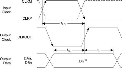
1. Dn = bits D0, D1, D2, and so forth, of channels A and B.
Figure 2. CMOS Interface Timing Diagram
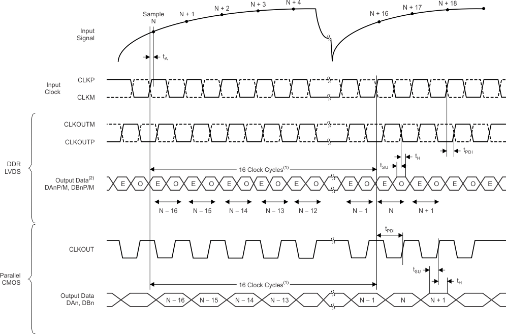
1. ADC latency after reset. At higher sampling frequencies, tPDI is greater than one clock cycle, which then makes the overall latency = ADC latency + 1.
2. E = even bits (D0, D2, D4, and so forth); O = odd bits (D1, D3, D5, and so forth).
Figure 3. Latency Timing Diagram
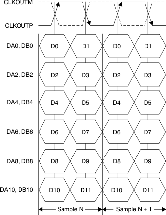 Figure 4. LVDS Interface Timing Diagram
7.11 Serial Interface Timing Characteristics
See (1).| PARAMETER | MIN | TYP | MAX | UNIT | |
|---|---|---|---|---|---|
| fSCLK | SCLK frequency (equal to 1/tSCLK) | > DC | 20 | MHz | |
| tSLOADS | SEN to SCLK setup time | 25 | ns | ||
| tSLOADH | SCLK to SEN hold time | 25 | ns | ||
| tDSU | SDATA setup time | 25 | ns | ||
| tDH | SDATA hold time | 25 | ns | ||
(1) Typical values at +25°C; minimum and maximum values across the full temperature range: TMIN = –40°C to TMAX = +85°C,
AVDD = 1.8 V, and DRVDD = 1.8 V, unless otherwise noted.
AVDD = 1.8 V, and DRVDD = 1.8 V, unless otherwise noted.
 Figure 5. Serial Interface Timing Diagram
7.12 Reset Timing (Only when Serial Interface is Used)
See (1).| PARAMETER | TEST CONDITIONS | MIN | TYP | MAX | UNIT | |
|---|---|---|---|---|---|---|
| t1 | Power-on delay | Delay from AVDD and DRVDD power-up to active RESET pulse | 1 | ms | ||
| t2 | Reset pulse width | Active RESET signal pulse width | 10 | ns | ||
| 1 | µs | |||||
| t3 | Register write delay | Delay from RESET disable to SEN active | 100 | ns | ||
(1) Typical values at +25°C; minimum and maximum values across the full temperature range: TMIN = –40°C to TMAX = +85°C, unless otherwise noted.
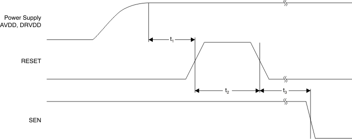
NOTE: A high pulse on the RESET pin is required in the serial interface mode when initialized through a hardware reset. For parallel interface operation, RESET must be permanently tied high.
Figure 6. Reset Timing Diagram
7.13 Typical Characteristics
7.13.1 Typical Characteristics: ADS4229
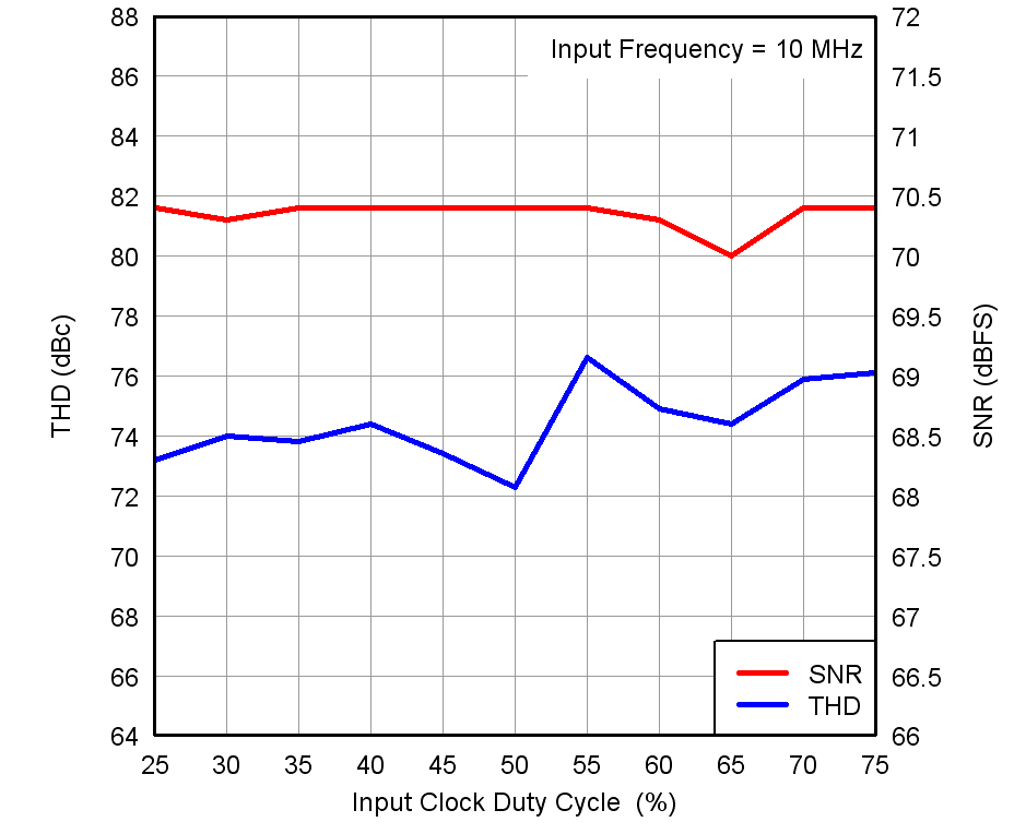
At TA = +25°C, AVDD = 1.8 V, DRVDD = 1.8 V, maximum rated sampling frequency, sine wave input clock, 1.5 VPP differential clock amplitude, 50% clock duty cycle, –1-dBFS differential analog input, High-Performance Mode enabled, 0-dB gain, DDR LVDS output interface, and 32k point FFT, unless otherwise noted.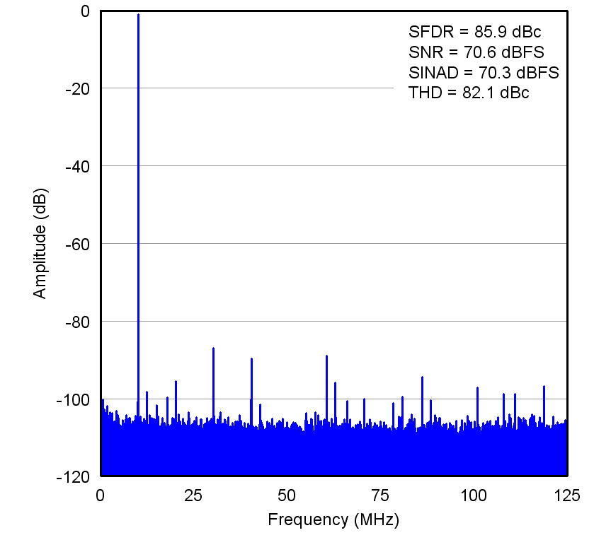 Figure 7. Input Signal (10 MHz)
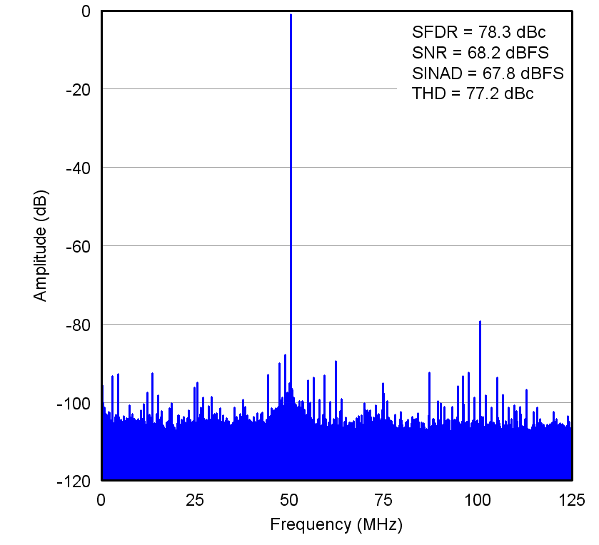 Figure 9. Input Signal (300 MHz)
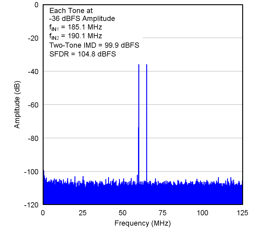 Figure 11. Two-Tone Input Signal
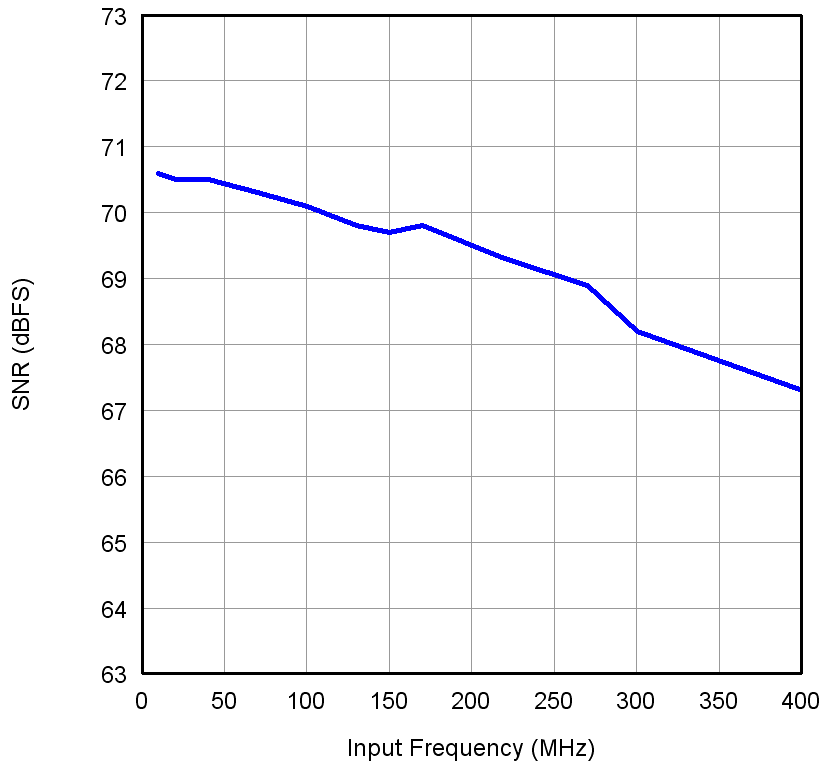 Figure 13. SNR vs Input Frequency
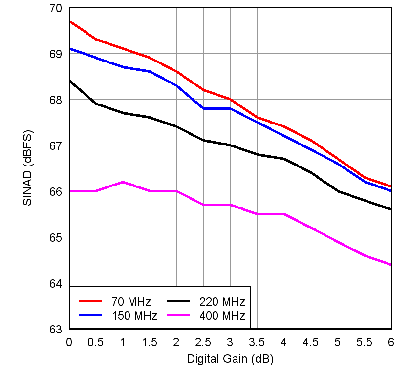 Figure 15. SINAD vs Gain and Input Frequency
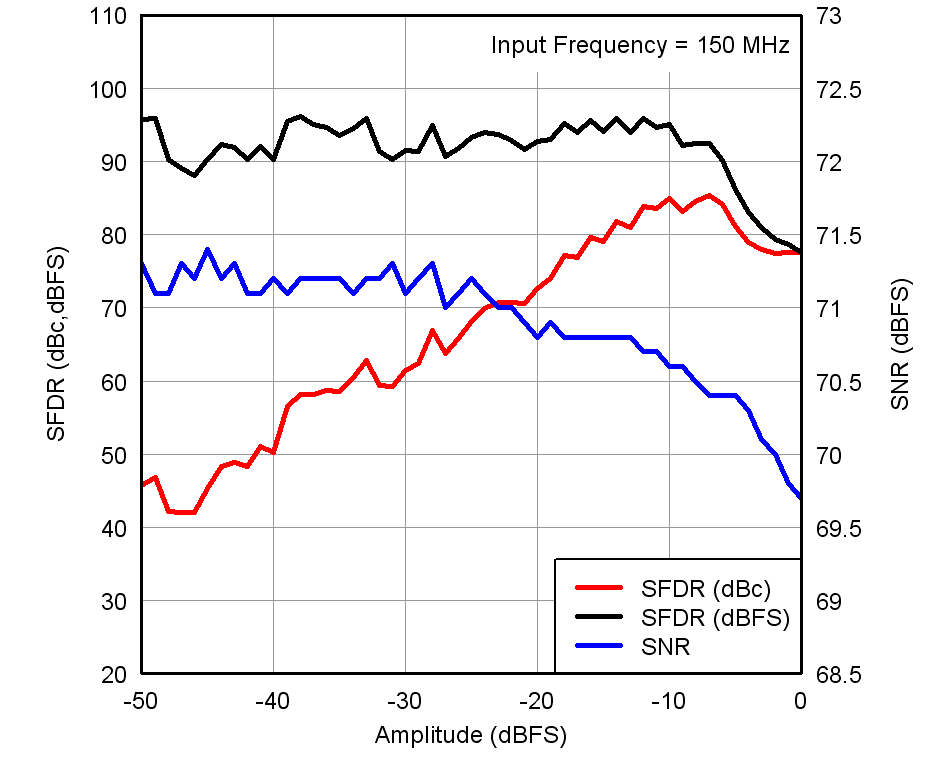 Figure 17. Performance vs Input Amplitude
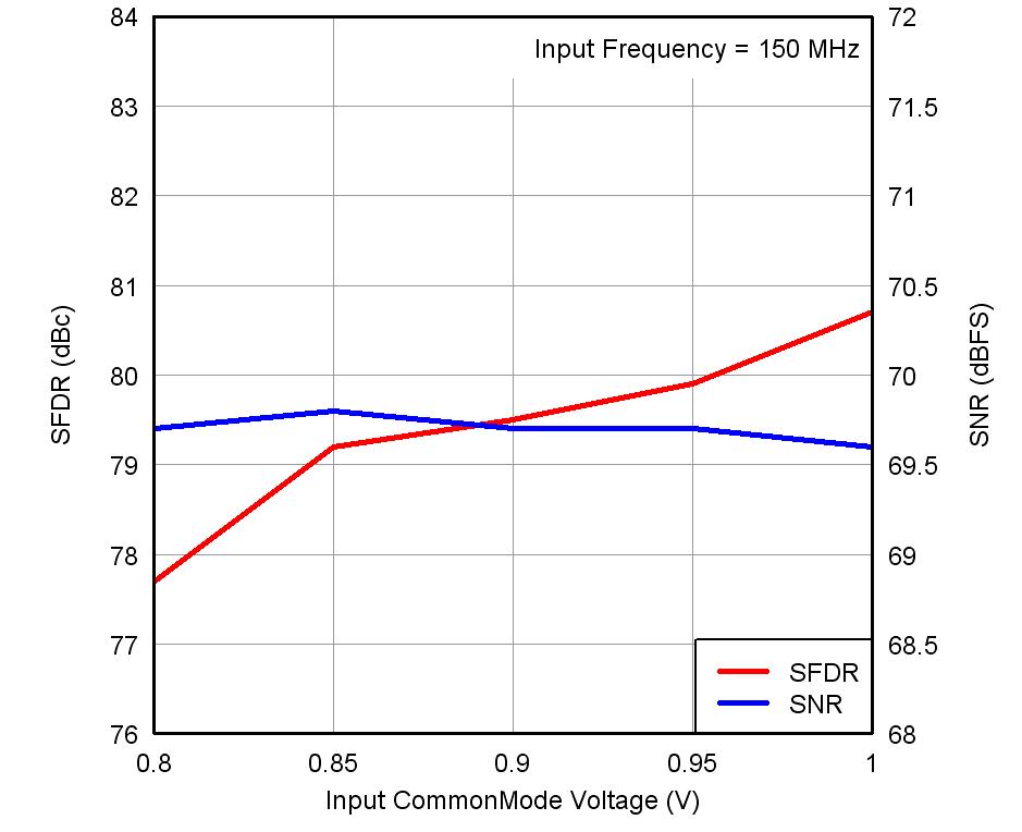 Figure 19. Performance vs Input Common-Mode Voltage
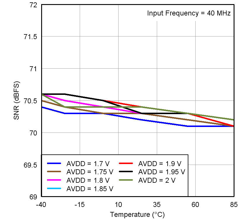 Figure 21. SNR vs Temperature and AVDD Supply
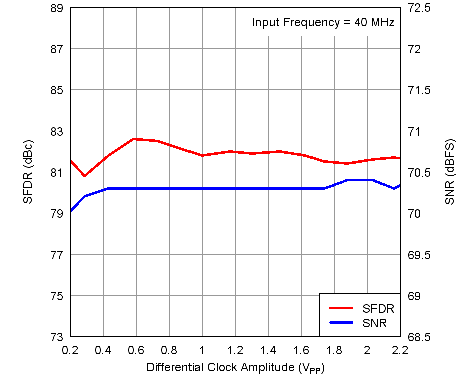 Figure 23. Performance vs Input Clock Amplitude
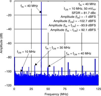 Figure 27. CMRR Plot
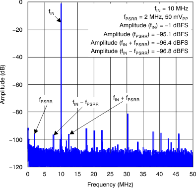 Figure 29. PSRR Plot
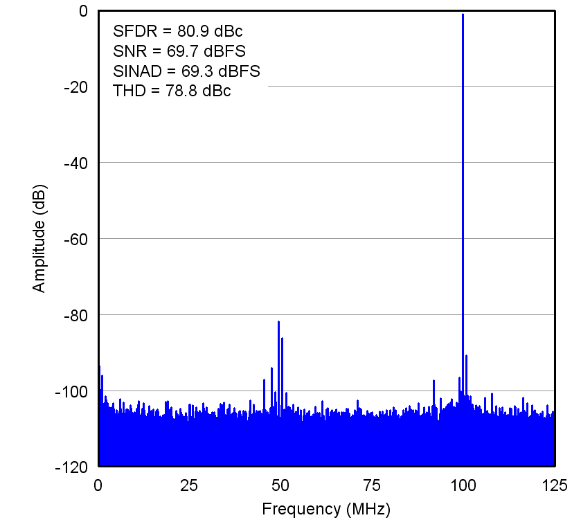 Figure 8. Input Signal (150 MHz)
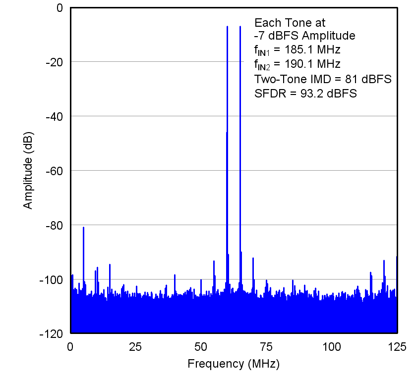 Figure 10. Two-Tone Input Signal
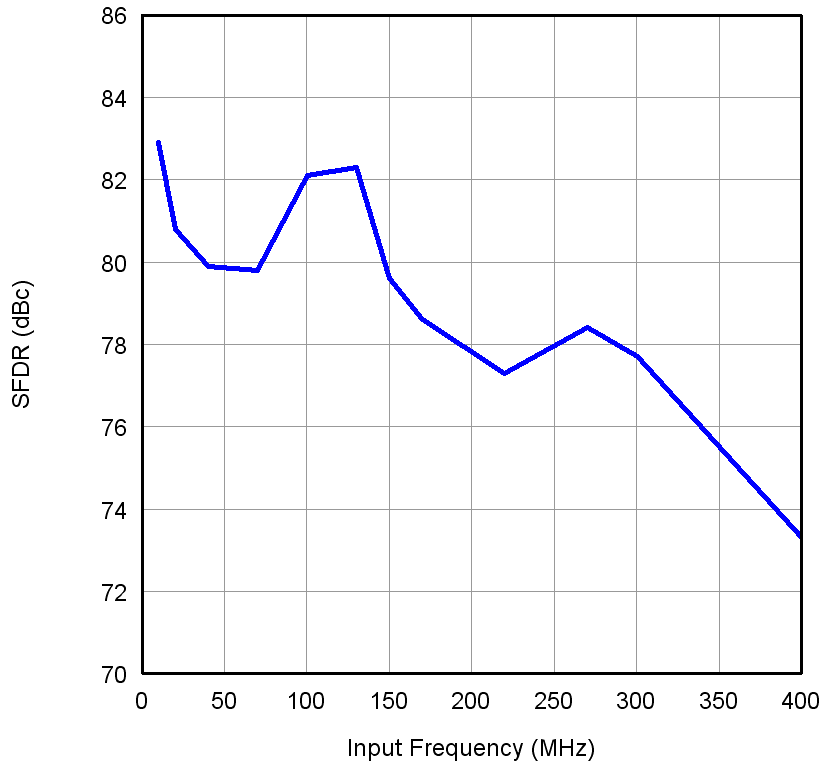 Figure 12. SFDR vs Input Frequency
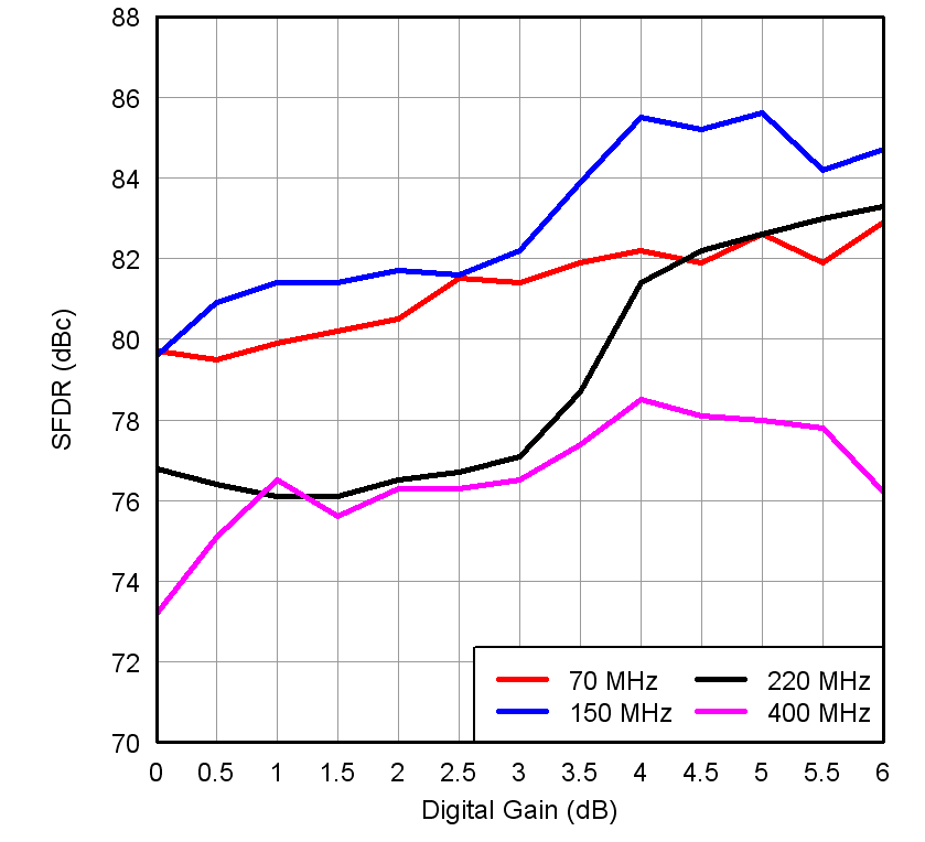 Figure 14. SFDR vs Gain and Input Frequency
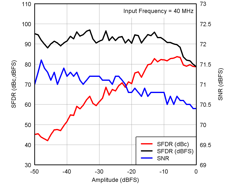 Figure 16. Performance vs Input Amplitude
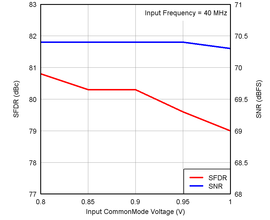 Figure 18. Performance vs Input Common-Mode Voltage
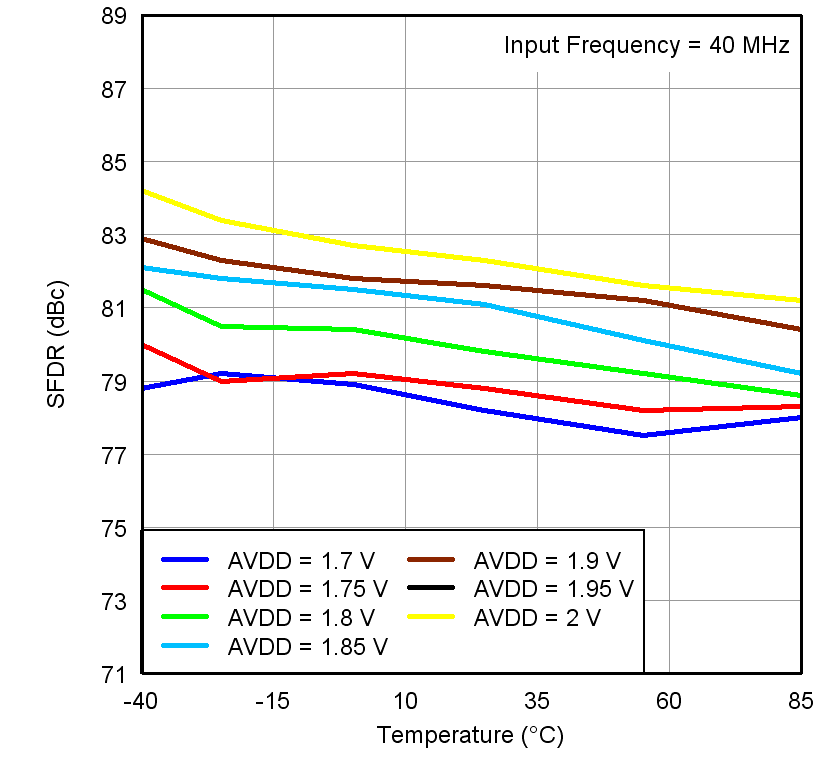 Figure 20. SFDR vs Temperature and AVDD Supply
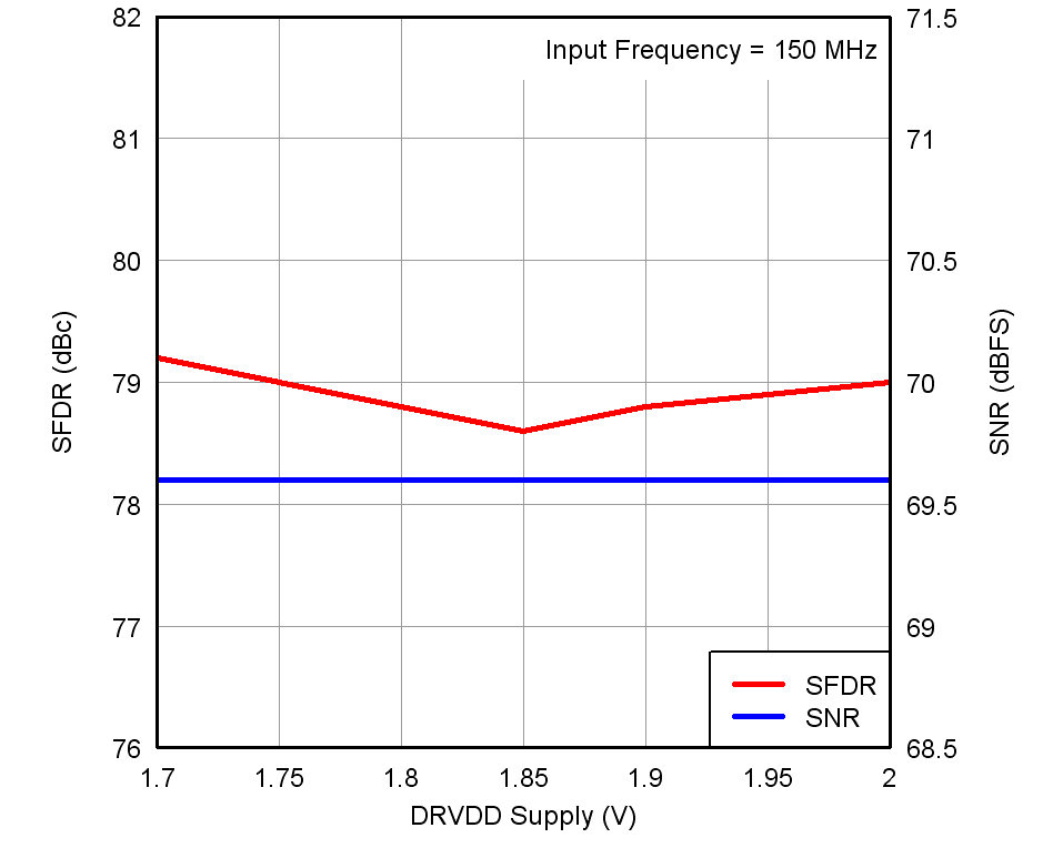 Figure 22. Performance vs DRVDD Supply Voltage
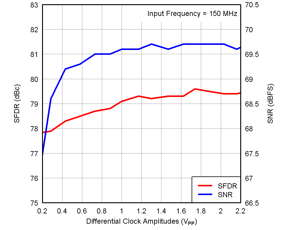 Figure 24. Performance vs Input Clock Amplitude
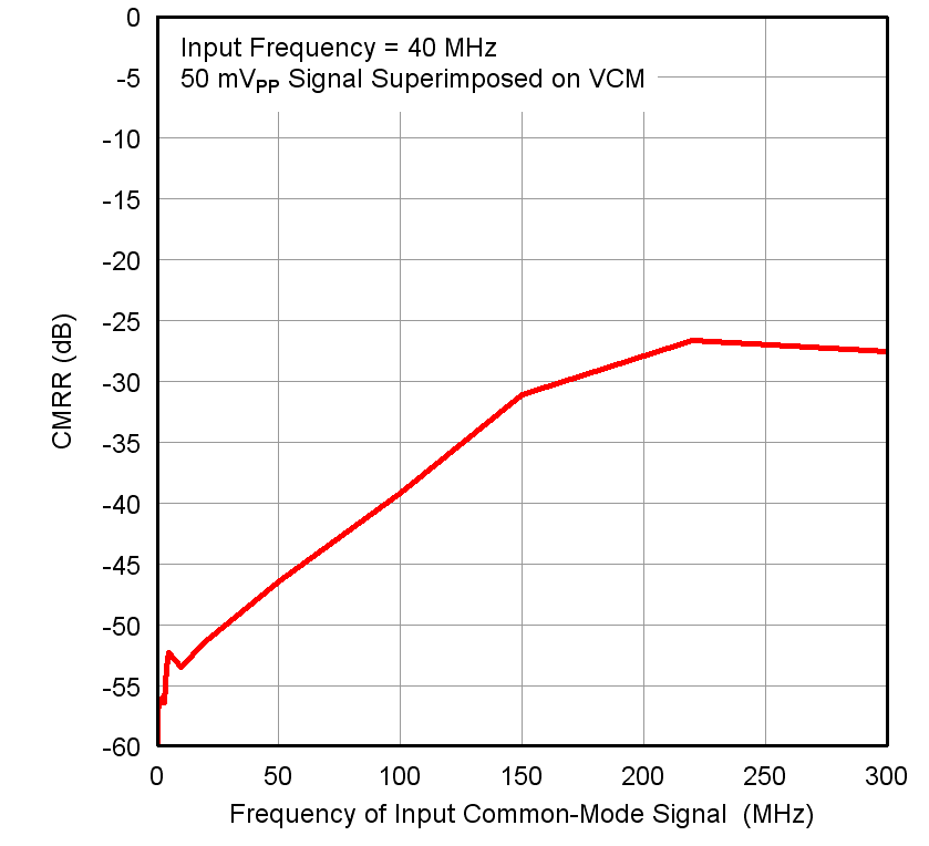 Figure 26. CMRR vs Test Signal Frequency
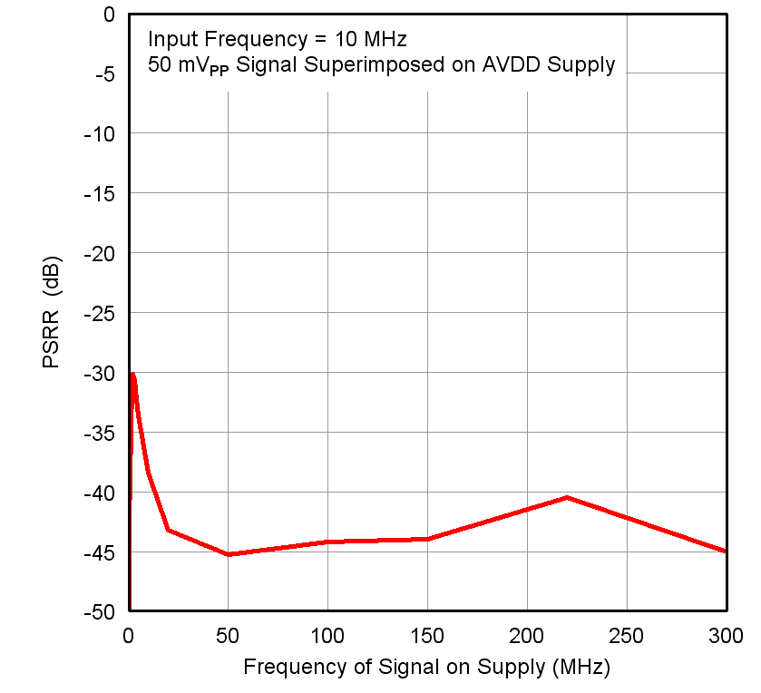 Figure 28. PSRR vs Test Signal Frequency
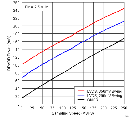
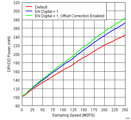
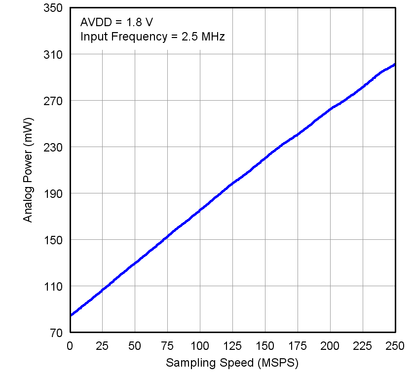 Figure 30. Analog Power vs Sampling Frequency
7.13.2 Typical Characteristics: Contour
All graphs are at +25°C, AVDD = 1.8 V, DRVDD = 1.8 V, maximum rated sampling frequency, sine wave input clock. 1.5 VPP differential clock amplitude, 50% clock duty cycle, –1-dBFS differential analog input, High-Performance Mode enabled, 0-dB gain, DDR LVDS output interface, and 32k point FFT, unless otherwise noted.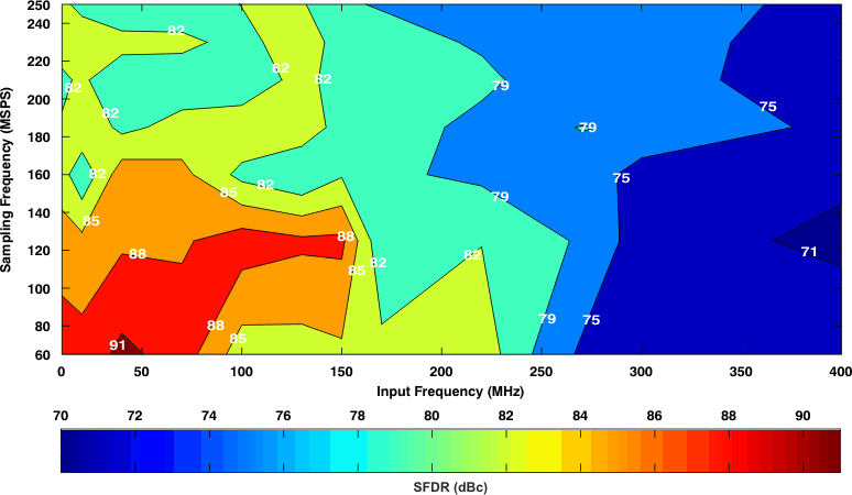 Figure 33. Spurious-Free Dynamic Range (0-dB Gain)
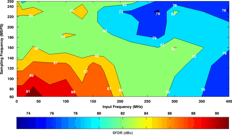 Figure 34. Spurious-Free Dynamic Range (6-dB Gain)
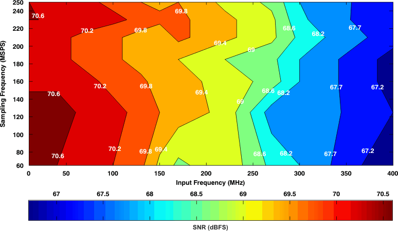 Figure 35. Signal-to-Noise Ratio (0-dB Gain)
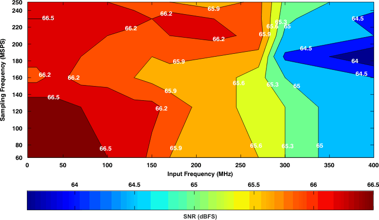 Figure 36. Signal-to-Noise Ratio (6-dB Gain)
