SBAS559B May 2022 – November 2025 ADS1285
PRODUCTION DATA
- 1
- 1 Features
- 2 Applications
- 3 Description
- 4 Pin Configuration and Functions
-
5 Specifications
- 5.1 Absolute Maximum Ratings
- 5.2 ESD Ratings
- 5.3 Recommended Operating Conditions
- 5.4 Thermal Information
- 5.5 Electrical Characteristics
- 5.6 Timing Requirements: 1.65V ≤ IOVDD ≤ 1.95V and 2.7V ≤ IOVDD ≤ 3.6V
- 5.7 Switching Characteristics: 1.65V ≤ IOVDD ≤ 1.95V and 2.7V ≤ IOVDD ≤ 3.6V
- 5.8 Timing Diagrams
- 5.9 Typical Characteristics
- 6 Parameter Measurement Information
-
7 Detailed Description
- 7.1 Overview
- 7.2 Functional Block Diagram
- 7.3 Feature Description
- 7.4 Device Functional Modes
- 7.5
Programming
- 7.5.1 Serial Interface
- 7.5.2 Conversion Data Format
- 7.5.3
Commands
- 7.5.3.1 Single Byte Command
- 7.5.3.2 WAKEUP: Wake Command
- 7.5.3.3 STANDBY: Software Power-Down Command
- 7.5.3.4 SYNC: Synchronize Command
- 7.5.3.5 RESET: Reset Command
- 7.5.3.6 Read Data Direct
- 7.5.3.7 RDATA: Read Conversion Data Command
- 7.5.3.8 RREG: Read Register Command
- 7.5.3.9 WREG: Write Register Command
- 7.5.3.10 OFSCAL: Offset Calibration Command
- 7.5.3.11 GANCAL: Gain Calibration Command
- 7.6
Register Map
- 7.6.1
Register Descriptions
- 7.6.1.1 ID/SYNC: Device ID, SYNC Register (Address = 00h) [Reset = xxxx0000b]
- 7.6.1.2 CONFIG0: Configuration Register 0 (Address = 01h) [Reset = 12h]
- 7.6.1.3 CONFIG1: Configuration Register 1 (Address = 02h) [Reset = 00h]
- 7.6.1.4 HPF0, HPF1: High-Pass Filter Registers (Address = 03h, 04h) [Reset = 32h, 03h]
- 7.6.1.5 OFFSET0, OFFSET1, OFFSET2: Offset Calibration Registers (Address = 05h, 06h, 07h) [Reset = 00h, 00h, 00h]
- 7.6.1.6 GAIN0, GAIN1, GAIN2: Gain Calibration Registers (Address = 08h, 09h, 0Ah) [Reset = 00h, 00h, 40h]
- 7.6.1.7 GPIO: Digital Input/Output Register (Address = 0Bh) [Reset = 000xx000b]
- 7.6.1.8 SRC0, SRC1: Sample Rate Converter Registers (Address = 0Ch, 0Dh) [Reset = 00h, 80h]
- 7.6.1
Register Descriptions
- 8 Application and Implementation
- 9 Device and Documentation Support
- 10Revision History
- 11Mechanical, Packaging, and Orderable Information
3 Description
The ADS1285 is a 32-bit, low-power, analog-to-digital converter (ADC), with a programmable gain amplifier (PGA) and a finite impulse response (FIR) filter. The ADC is designed for the demanding needs of seismology equipment requiring low-noise precision digitization and extended battery run time.
The low-noise PGA allows direct connection of geophones and transformer-coupled hydrophones without the need of an external amplifier.
The ADC incorporates a high-resolution, delta-sigma (ΔΣ) modulator and a FIR filter with programmable phase response. The high-pass filter removes dc and low-frequency content from the signal. Clock frequency error is compensated by the sample rate converter with 7ppb resolution.
Choice of power modes optimize dynamic range verses power consumption. Power consumption is further reduced by PGA bypass operation.
The ADC is available in a compact 5mm × 5mm VQFN package and is fully specified over the –40°C to +85°C ambient temperature range.
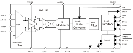 Functional Block Diagram