SBAS951B August 2019 – April 2020 AMC1336
PRODUCTION DATA.
- 1 Features
- 2 Applications
- 3 Description
- 4 Revision History
- 5 Pin Configuration and Functions
-
6 Specifications
- Table 1. Absolute Maximum Ratings
- Table 2. ESD Ratings
- Table 3. Recommended Operating Conditions
- Table 4. Thermal Information
- Table 5. Power Ratings
- Table 6. Insulation Specifications
- Table 7. Safety-Related Certifications
- Table 8. Safety Limiting Values
- Table 9. Electrical Characteristics
- Table 10. Switching Characteristics
- 6.1 Insulation Characteristics Curves
- 6.2 Typical Characteristics
- 7 Detailed Description
- 8 Application and Implementation
- 9 Power Supply Recommendations
- 10Layout
- 11Device and Documentation Support
- 12Mechanical, Packaging, and Orderable Information
7.3.5 Digital Output
A differential input signal of 0 V ideally produces a stream of ones and zeros that are high 50% of the time. A differential input of 1 V produces a stream of ones and zeros that are high 90% of the time. With 16 bits of resolution, that percentage ideally corresponds to code 58982 (an unsigned code). A differential input of –1 V produces a stream of ones and zeros that are high 10% of the time and ideally results in code 6553 with 16-bit resolution. These input voltages are also the specified linear range of the AMC1336 with performance as specified in this document. If the input voltage value exceeds this range, the output of the modulator shows nonlinear behavior when the quantization noise increases. The output of the modulator clips with a stream of only zeros with an input less than or equal to –1.25 V or with a stream of only ones with an input greater than or equal to 1.25 V. In this case, however, the AMC1336 generates a single 1 (if the input is at negative full-scale) or 0 every 128 clock cycles to indicate proper device function (see the AVDD Diagnostics and Fail-Safe Output section for more details). Figure 45 shows the input voltage versus the output modulator signal.
 Figure 45. Analog Input versus the AMC1336 Modulator Output
 Equation 1 calculates the density of ones in the output bitstream for any input voltage value (with the exception of a full-scale input signal, as described in theOutput Behavior in Case of a Full-Scale Input section):

The modulator bitstream on the DOUT pin changes with the rising edge of the clock signal applied on the CLKIN pin. Use the rising edge of the clock to latch the modulator bitstream at the input of the digital filter device.
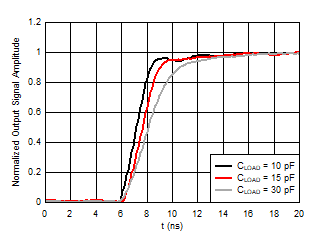
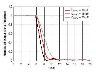
The AMC1336 features a slew-rate-controlled output stage that reduces the over- and undershoots of the output amplitude and radiated emissions of the DOUT line in the system. Figure 46 and Figure 47 show examples of rising and falling edges of DOUT with different capacitive loads.

