SBAU351 April   2021


  1.   Trademarks
  2. 1EVM Overview
    1. 1.1 ADS127L11EVM Kit
    2. 1.2 ADS127L11EVM Board
    3. 1.3 ADS127L11EVM-PDK-GUI Unsupported Features
  3. 2EVM Analog Interface
    1. 2.1 EVM Analog Input Options
    2. 2.2 ADC Connections and Decoupling
    3. 2.3 ADC Input Drive Amplifiers
    4. 2.4 VCOM Buffer
    5. 2.5 Onboard Voltage Reference
    6. 2.6 External Voltage Reference
    7. 2.7 Clock Tree
  4. 3Digital Interface
    1. 3.1 Serial Interface (SPI)
    2. 3.2 I2C Bus for Onboard EEPROM
  5. 4Power Supplies
    1. 4.1 Power Connection and Configuration
    2. 4.2 Low Dropout Regulator (LDO)
  6. 5ADS127L11EVM Software Installation
  7. 6EVM Operation
    1. 6.1 Connecting the Hardware
    2. 6.2 Optional Connections to the EVM
    3. 6.3 EVM GUI Global Settings for ADC Control
    4. 6.4 Time Domain Display
    5. 6.5 Frequency Domain Display
    6. 6.6 Histogram Display
  8. 7Bill of Materials, Schematics, and Layout
    1. 7.1 Bill of Materials
    2. 7.2 Board Layouts
    3. 7.3 Schematics
  9. 8References

Serial Interface (SPI)

The ADS127L11 ADC uses SPI serial communication in mode 1 (CPOL = 0, CPHA = 1). Because the serial clock (SCLK) frequency can be as fast as 40 MHz, the ADS127L11 EVM offers 10-Ω resistors between the SPI signals to aid with signal integrity. Typically, in high-speed SPI communication, fast signal edges can cause overshoot; these 10-Ω resistors slow down the signal edges in order to minimize signal overshoot. J2 provides test points to measure the digital signals.
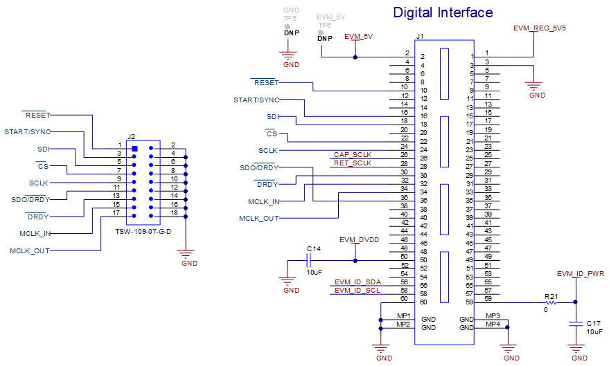
GUID-26DFB47C-509B-40CA-A233-76D786D36C07-low.gifFigure 3-1 Connection to Digital Signals on PHI and Test Points