SBAU361 December   2020 ADC3664


  1.   Trademarks
  2. 1Introduction
  3. 2Equipment
    1. 2.1 ADC3664EVM Functionality
    2. 2.2 Evaluation Board Feature Identification Summary
    3. 2.3 Required Equipment
  4. 3Setup Procedure
    1. 3.1 Install High-Speed Data Converter (HSDC) Pro Software
    2. 3.2 Install ADC35XXEVM GUI 1.0 Software
    3. 3.3 Connect the ADC3664 EVM and TSW1400EVM
    4. 3.4 Connect the Power Supply and Mini-USB Connections
    5. 3.5 Connect the Clocks and Analog Input
  5. 4Device Configuration
    1. 4.1 Bypass Mode
      1. 4.1.1 ADC35XX GUI: Bypass Mode Configuration
      2. 4.1.2 HSDC Pro: Bypass Mode
    2. 4.2 Real Decimation Mode
      1. 4.2.1 ADC35XX GUI: Real Decimation Mode Configuration
      2. 4.2.2 HSDC Pro: Real Decimation Mode
    3. 4.3 Complex Decimation Mode
      1. 4.3.1 ADC35XX GUI: Complex Decimation Configuration
      2. 4.3.2 HSDC PRO: Complex Decimation Mode
  6. 5Onboard FDA Configuration
  7. 6ADC3664EVM Power Monitor
  8. 7Test Pattern

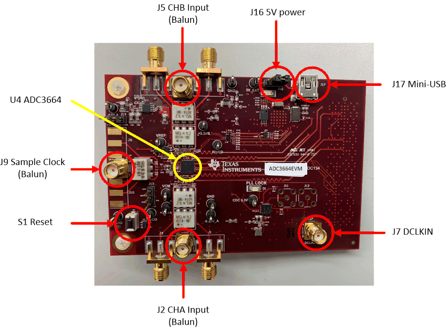
Evaluation Board Feature Identification Summary

GUID-20201203-CA0I-WHM1-V1GN-MGW9LXXTQKDX-low.gif Figure 2-3 ADC3664EVM Feature Identification

Ensure that jumper J16 is shunted in the 2-3 position. This allows 5 V to be supplied to the ADC3664EVM through the mini-USB connector.

If an external 5-V supply is desired, J16 must be shunted in the 1-2 position, and the external 5 V can be connected to the test point labeled "+5 EXT". The USB data connection will still be connected for SPI communications.

J13 is tied to the REFBUF pin. It can be left floating, or can be tied to 1.8 V (shunt pins 2-3) for normal operation.

J14 is tied to the PDN/SYNC pin. It can be left floating for tied to ground (shunt pins 1-2) for normal operation. To power down the ADC, tied to 1.8 V (shunt pins 2-3). The ADC may also be powered down via SPI.
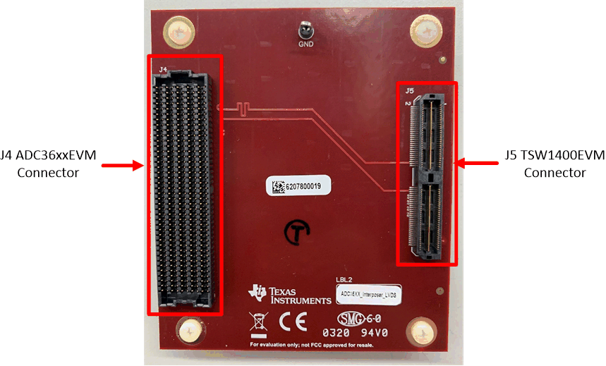
GUID-20201112-CA0I-BMTS-ZD4C-MT8S1ZVRVG2J-low.gif Figure 2-4 LVDS Interposer