SBOA212A January 2018 – January 2019 OPA2353 , OPA2365 , OPA353 , OPA365 , TLV3502
Design Goals
| Input | Output | Supply | ||||
|---|---|---|---|---|---|---|
| ViMin | ViMax | VoMin | VoMax | Vcc | Vee | Vref |
| –2.0 V | 2.0 V | 0 V | 5 V | 5 V | 0 V | 2.5 V |
Design Description
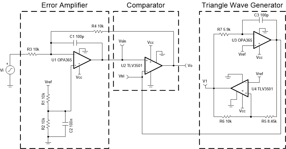
This circuit utilizes a triangle wave generator and comparator to generate a 500 kHz pulse-width-modulated (PWM) waveform with a duty cycle that is inversely proportional to the input voltage. An op amp and comparator (U3 and U4) generate a triangle waveform which is applied to the inverting input of a second comparator (U2). The input voltage is applied to the non-inverting input of U2. By comparing the input waveform to the triangle wave, a PWM waveform is produced. U2 is placed in the feedback loop of an error amplifier (U1) to improve the accuracy and linearity of the output waveform.
Design Notes
- Use a comparator with push-pull output and minimal propagation delay.
- Use an op amp with sufficient slew rate, GBW, and voltage output swing.
- Place the pole created by C1 below the switching frequency and well above the audio range.
- Vref must be low impedance (for example, output of an op amp).
Design Steps
- Set the error amplifier inverting
signal gain.
- Determine R1 and
R2 to divide Vref to cancel the non-inverting gain.
- The amplitude of Vtri
must be chosen such that it is greater than the maximum amplitude of
Vi (2.0 V) to avoid 0% or 100% duty cycle in the PWM output
signal. Select Vtri to be 2.1 V. The amplitude of V1 = 2.5
V.
- Set the oscillation frequency to
500 kHz.
- Choose C1 to limit
amplifier bandwidth to below switching frequency.
- Select C2 to filter noise from Vref.
Design Simulations
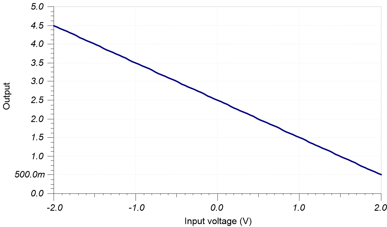
DC Simulation Results
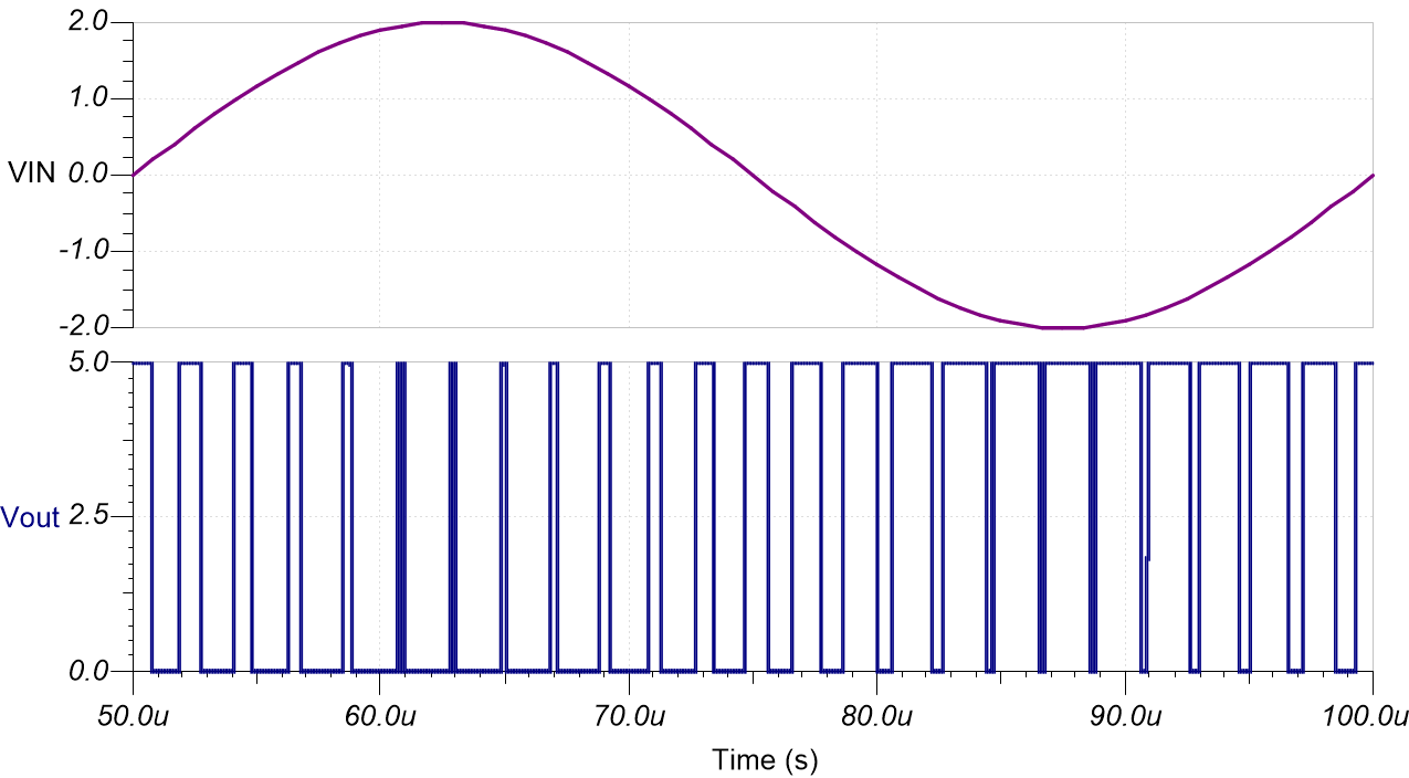
Transient Simulation Results
Design References
See Analog Engineer's Circuit Cookbooks for TI's comprehensive circuit library.
See circuit SPICE simulation file SBOC502.
See TIPD108, Analog PWM Generator 5V, 500 kHz PWM Output
Design Featured Op Amp
| OPA2365 | |
|---|---|
| Vss | 2.2 V to 5.5 V |
| VinCM | Rail-to-rail |
| Vout | Rail-to-rail |
| Vos | 100 µV |
| Iq | 4.6 mA |
| Ib | 2 pA |
| UGBW | 50 MHz |
| SR | 25 V/µs |
| #Channels | 2 |
| OPA2365 | |
Design Comparator
| TLV3502 | |
|---|---|
| Vss | 2.2 V to 5.5 V |
| VinCM | Rail-to-rail |
| Vout | Rail-to-rail |
| Vos | 1 mV |
| Iq | 3.2 mA |
| Ib | 2 pA |
| UGBW | — |
| SR | — |
| #Channels | 2 |
| TLV3502 | |
Design Alternate Op Amp
| OPA2353 | |
|---|---|
| Vss | 2.7 V to 5.5 V |
| VinCM | Rail-to-rail |
| Vout | Rail-to-rail |
| Vos | 3 mV |
| Iq | 5.2 mA |
| Ib | 0.5 pA |
| UGBW | 44 MHz |
| SR | 22 V/µs |
| #Channels | 2 |
| OPA2352 | |