SBOA271A january 2018 – january 2019 OPA171 , OPA191
Design Goals
| Input | Output | Supply | |||
|---|---|---|---|---|---|
| ViMin | ViMax | VoMin | VoMax | Vcc | Vee |
| –1 V | 1 V | –10 V | 10 V | 15 V | –15 V |
Design Description
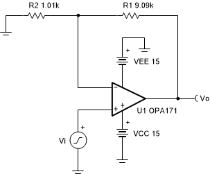
This design amplifies the input signal, Vi, with a signal gain of 10 V/V. The input signal may come from a high-impedance source (for example, MΩ) because the input impedance of this circuit is determined by the extremely high input impedance of the op amp (for example, GΩ). The common-mode voltage of a non-inverting amplifier is equal to the input signal.
Design Notes
- Use the op amp linear output operating range, which is usually specified under the AOL test conditions. The common-mode voltage is equal to the input signal.
- The input impedance of this circuit is equal to the input impedance of the amplifier.
- Using high-value resistors can degrade the phase margin of the circuit and introduce additional noise in the circuit.
- Avoid placing capacitive loads directly on the output of the amplifier to minimize stability issues.
- The small-signal bandwidth of a non-inverting amplifier depends on the gain of the circuit and the gain bandwidth product (GBP) of the amplifier. Additional filtering can be accomplished by adding a capacitor in parallel to R1. Adding a capacitor in parallel with R1 will also improve stability of the circuit if high-value resistors are used.
- Large signal performance may be limited by slew rate. Therefore, check the maximum output swing versus frequency plot in the data sheet to minimize slew-induced distortion.
- For more information on op amp linear operating region, stability, slew-induced distortion, capacitive load drive, driving ADCs, and bandwidth please see the Design References section.
Design Steps
The transfer function for this circuit is given below.
- Calculate the gain.
- Calculate values for R1 and R2.
- Calculate the minimum slew rate required to minimize slew-induced distortion.
- The slew rate of the OPA171 is 1.5 V/µs, therefore it meets this requirement.
- To maintain sufficient phase margin, ensure that the zero created by the gain setting resistors and input capacitance of the device is greater than the bandwidth of the circuit.
- Ccm and Cdiff are the common-mode and differential input capacitances of the OPA171, respectively.
- Since the zero frequency is greater than the bandwidth of the circuit, this requirement is met.
Design Simulations
DC Simulation Results
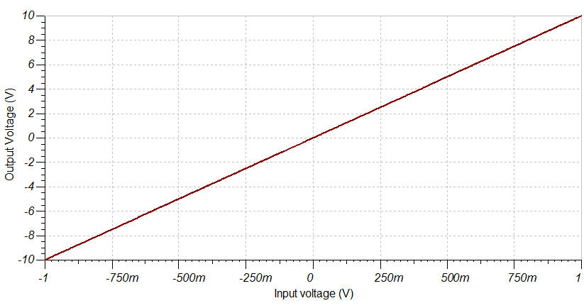
AC Simulation Results
Design References
See Analog Engineer's Circuit Cookbooks for TI's comprehensive circuit library.
See circuit SPICE simulation file SBOC493.
For more information on many op amp topics including common-mode range, output swing, and bandwidth please visit TI Precision Labs.
Design Featured Op Amp
| OPA171 | |
|---|---|
| Vss | 2.7 V to 36 V |
| VinCM | (Vee–0.1 V) to (Vcc–2 V) |
| Vout | Rail-to-rail |
| Vos | 250 µV |
| Iq | 475 µA |
| Ib | 8 pA |
| UGBW | 3 MHz |
| SR | 1.5 V/µs |
| #Channels | 1, 2, and 4 |
| OPA171 | |
Design Alternate Op Amp
| OPA191 | |
|---|---|
| Vss | 4.5 V to 36 V |
| VinCM | Rail-to-rail |
| Vout | Rail-to-rail |
| Vos | 5 µV |
| Iq | 140 µA |
| Ib | 5 pA |
| UGBW | 2.5 MHz |
| SR | 7.5 V/µs |
| #Channels | 1, 2, and 4 |
| OPA191 | |