SBOA274A february 2018 – january 2019 OPA320 , TLV6001
Design Goals
| Input (Vi2-Vi1) | Output | CMRR (min) | Supply | ||||
|---|---|---|---|---|---|---|---|
| VidiffMin | VidiffMax | VoMin | VoMax | dB | Vcc | Vee | Vref |
| –1.25 V | 1.25 V | –2.5 V | 2.5 V | 50 | 2.75 V | –2.75 V | 0 V |
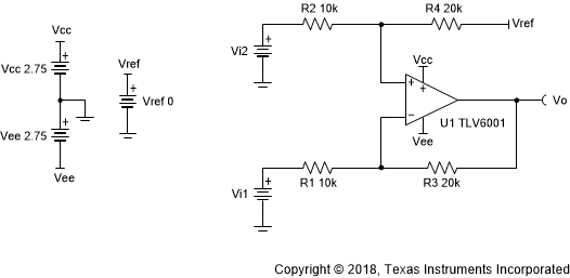
Design Description
This design inputs two signals, Vi1 and Vi2, and outputs their difference (subtracts). The input signals typically come from low-impedance sources because the input impedance of this circuit is determined by the resistive network. Difference amplifiers are typically used to amplify differential input signals and reject common-mode voltages. A common-mode voltage is the voltage common to both inputs. The effectiveness of the ability of a difference amplifier to reject a common-mode signal is known as common-mode rejection ratio (CMRR). The CMRR of a difference amplifier is dominated by the tolerance of the resistors.
Design Notes
- Use the op amp in a linear operating region. Ensure that the inputs of the op amp do not exceed the common-mode range of the device. Linear output swing is usually specified under the AOL test conditions.
- The input impedance is determined by the input resistive network. Make sure these values are large when compared to the output impedance of the sources.
- Using high-value resistors can degrade the phase margin of the circuit and introduce additional noise in the circuit.
- Avoid placing capacitive loads directly on the output of the amplifier to minimize stability issues.
- Small-signal bandwidth is determined by the noise gain (or non-inverting gain) and op amp gain-bandwidth product (GBP). Additional filtering can be accomplished by adding a capacitors in parallel to R3 and R4. Adding capacitors in parallel with R3 and R4 will also improve stability of the circuit if high-value resistors are used.
- Large signal performance may be limited by slew rate. Therefore, check the maximum output swing versus frequency plot in the data sheet to minimize slew-induced distortion.
- For more information on op amp linear operating region, stability, slew-induced distortion, capacitive load drive, driving ADCs, and bandwidth please see the Design References section.
Design Steps
The complete transfer function for this circuit is shown below.
If R1 = R2 and R3 = R4 the transfer function for this circuit simplifies to the following equation.
- Where the gain, G, is R3/R1.
- Determine the starting value of R1 and R2. The relative size of R1 and R2 to the signal impedance of the source affects the gain error.
- Calculate the gain required for the circuit.
- Calculate the values for R3 and R4.
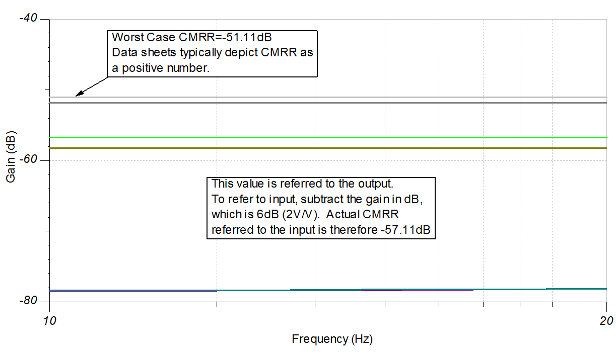
- Calculate resistor tolerance to meet the minimum common-mode rejection ratio (CMRR). For minimum (worst-case) CMRR, α = 4. For a more probable, or typical value of CMRR, α = 0.33.
- For quick reference, the following table compares resistor tolerance to minimum and typical CMRR values assuming G = 1 or G = 2. As shown above, as gain increases so does CMRR.
Tolerance G=1 Minimum (dB) G=1 Typical (dB) G=2 Minimum (dB) G=2 Typical (dB) 0.01%=0.0001 74 95.6 77.5 99.2 0.1%=0.001 54 75.6 57.5 79.2 0.5%=0.005 40 61.6 43.5 65.2 1%=0.01 34 55.6 37.5 59.2 5%=0.05 20 41.6 23.5 45.2
Design Simulations
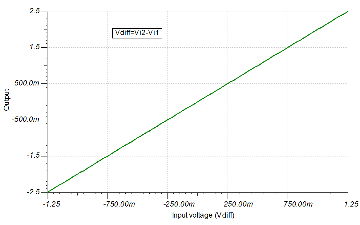
DC Simulation Results
CMRR Simulation Results
Design References
See Analog Engineer's Circuit Cookbooks for TI's comprehensive circuit library.
See circuit SPICE simulation file SBOC495.
For more information on many op amp topics including common-mode range, output swing, bandwidth, and how to drive an ADC please visit TI Precision Labs. For more information on difference amplifier CMRR, please read Overlooking the obvious: the input impedance of a difference amplifier.
Design Featured Op Amp
| TLV6001 | |
|---|---|
| Vss | 1.8 V to 5.5 V |
| VinCM | Rail-to-rail |
| Vout | Rail-to-rail |
| Vos | 750 µV |
| Iq | 75 µA |
| Ib | 1 pA |
| UGBW | 1 MHz |
| SR | 0.5 V/µs |
| #Channels | 1, 2, and 4 |
| TLV6001 | |
Design Alternate Op Amp
| OPA320 | |
|---|---|
| Vss | 1.8 V to 5.5 V |
| VinCM | Rail-to-rail |
| Vout | Rail-to-rail |
| Vos | 40 µV |
| Iq | 1.5 mA |
| Ib | 0.2 pA |
| UGBW | 20 MHz |
| SR | 10 V/µs |
| #Channels | 1 and 2 |
| OPA320 | |