SBOA313A July 2018 – August 2019 TLV7031
Design Goals
| Output | Thresholds | Supply | |||||
|---|---|---|---|---|---|---|---|
| Vo = HIGH | Vo = LOW | VH | VL | VHYS | Vcc | Vpu | Vref |
| Vi > VH | Vi < VL | 1.7 V | 1.3 V | 400 mV | 3 V | 3 V | 3 V |
Design Description
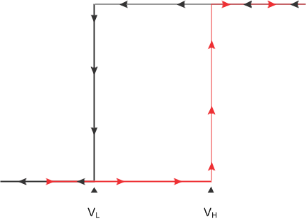
Comparators are used to differentiate between two different signal levels. With noise, signal variation, or slow-moving signals, undesirable transitions at the output can be observed with a constant threshold. Setting upper and lower hysteresis thresholds eliminates these undesirable output transitions. This circuit example will focus on the steps required to design the positive feedback resistor network necessary to obtain the desired hysteresis for a non-inverting comparator application.
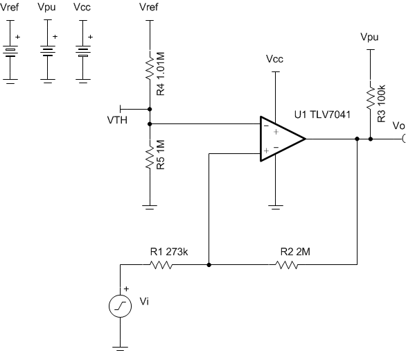
Design Notes
- The accuracy of the hysteresis threshold voltages are related to the tolerance of the resistors used in the circuit, the selected comparator’s input offset voltage specification, and any internal hysteresis of the device.
- The TLV7041 has an open-drain output stage, so a pull-up resistor is needed.
Design Steps
- Select the switching thresholds for
when the comparator will transition from high to low (VL) and low to
high (VH). VL is the necessary input voltage for the
comparator output to transition low and VH is the required input
voltage for the comparator to output high.
- Analyze the circuit when the input
voltage is VH. At this point, Vo=0V and the transition to
a logic high is initiated in the comparator output. Solve for the voltage seen
by the comparator's non-inverting pin, VTH.
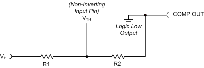
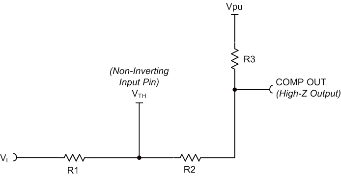
- Analyze the circuit when the input
voltage is VL. At this point, Vo=Vpu (or
Vo=Vcc if the comparator has a push-pull output stage)
and the transition to a logic low is initiated in the comparator output. Using
superposition, solve for VTH.
- Set R2 to be large for
power conservation. This resistance can be changed to meet certain design
specifications but it was selected to be 2 MΩ. Now set the two VTH
equations equal and solve for R1.
- Calculate
VTH using the equation derived in step 2.
- Assuming a value for R5
of 1 MΩ for reduced power consumption, calculate R4 using the
following relationship developed from a basic voltage divider of the reference
voltage VREF. The voltage at the inverting terminal is
VTH.
Design Simulations
DC Transfer Simulation Results
Transient Simulation Results
Design References
See Analog Engineer's Circuit Cookbooks for TI's comprehensive circuit library.
See Circuit SPICE Simulation File SLVMCR2.
For more information on many comparator topics including hysteresis, propagation delay and input common mode range please see TI Precision Labs - Op amps.
Design Featured Comparator
| TLV7031, TLV7041 | |
|---|---|
| Output Type | PP (7031), OD (7041) |
| Vcc | 1.6 V to 6.5 V |
| VinCM | Rail-to-rail |
| Vos | ±100 µV |
| VHYS | 7 mV |
| Iq | 335 nA/Ch |
| tpd | 3 µs |
| #Channels | 1 and 2 |
| TLV7041 Product Page | |
Design Alternate Comparator
| TLV1701 | TLV7011, TLV7011 | |
|---|---|---|
| Output Type | Open Collector | PP (7011), OD (7021) |
| Vcc | 2.2 V to 36 V | 1.6 V to 5.5 V |
| VinCM | Rail-to-rail | Rail-to-rail |
| VHYS | N/A | 4.2 mV |
| Vos | ±500 µV | ±500 µV |
| Iq | 55 µA/Ch | 335 nA/Ch |
| tpd | 560 ns | 3 µs |
| #Channels | 1, 2, and 4 | 1 and 2 |
| TLV1701 Product Page | TLV7011 Product Page |