SBOA436 October 2020 OPA192
Design Steps
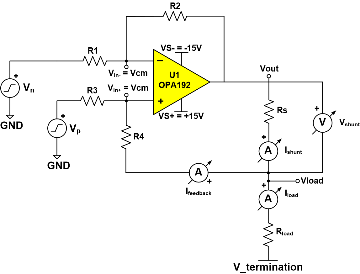
Calculating gain (G) for a given Iload and shunt resistor:
Equation 1.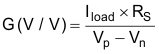 Equation 1.
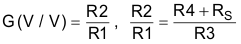
Ensure Vout is within the voltage output swing from rails (Vout_Min, Vout_Max) of the op amp at a specific output current specified in the data sheet of the op amp:
Equation 1.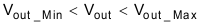 Equation 1.