SBOA441 October 2020 OPA192 , OPA2192
Design Steps
Calculating gain (G) for a given Iload and shunt resistor:
Equation 1.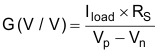 Equation 1.
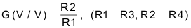
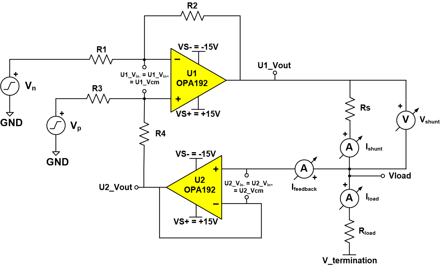
Ensure Vout for both op amps are within their voltage output swing from rails (Vout_Min, Vout_Max) at a specific output current specified in the data sheet.The following formula can be used to calculate U1_Vout for U1 OPA192. U2_Vout for U2 OPA192 will be Vload.
Equation 1.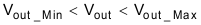 Equation 1.