SBOA535 February 2022 INA190
3.1 Unsuccessful Design With a Single Device
When designing amplifiers into the microamp range, one design aspect that must be considered is the input bias currents of the amplifier. As these currents will ultimately flow through the shunt to enter the IN– leg of the amplifier, the designer is restricted to amplifiers that exhibit input bias currents far less than the minimum desired measurement point. As such, the best choice from the TI portfolio for a design needing to measure microamps is the INA190, which has a worst-case bias current magnitude of 3 nA, which should minimize the impact of this error on the lower range. The sheer magnitude of this dynamic range (10000:1) presents an issue, however.
For the INA190, the maximum output achievable due to worst-case swing-to-rail limitation is 4.96 V, and thus for a 100-mA maximum measurement, the maximum possible calculated shunt is 1.984 Ω.
For the given conditions, Figure 3-1 gives the overall output error curve for the design utilizing this shunt, while Figure 3-2 examines the error curve only down to 0.1 mA, for better granularity.
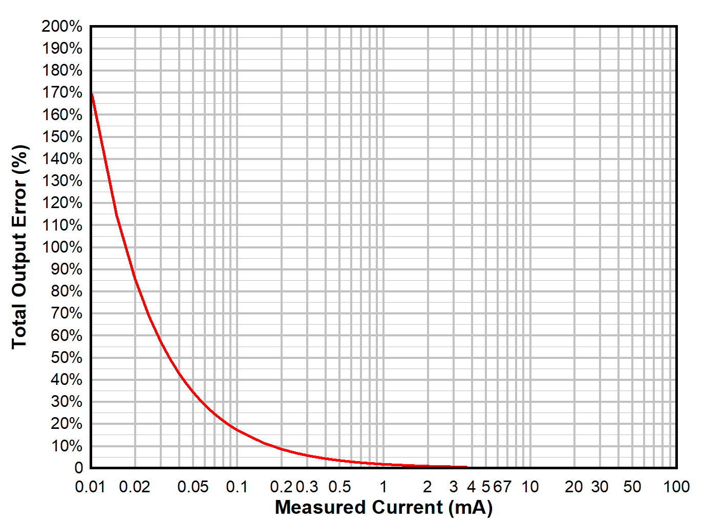 Figure 3-1 Total Output Error (%) Over
Measurement Range, RSHUNT = 1.984 Ω, 10 µA to 100 mA, Ideal Shunt
Tolerance
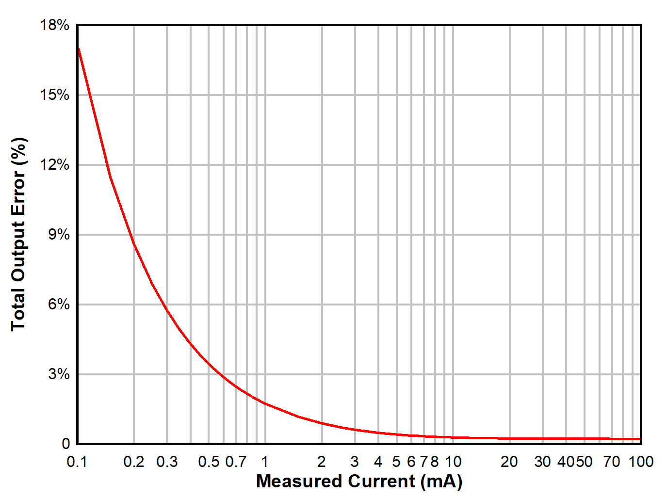 Figure 3-2 Total Output Error (%) Over
Measurement Range, RSHUNT = 1.984 Ω, 100 µA to 100 mA, Ideal Shunt
Tolerance
Figure 3-2 Total Output Error (%) Over
Measurement Range, RSHUNT = 1.984 Ω, 100 µA to 100 mA, Ideal Shunt
ToleranceFrom the latter curve, it is observed that the utilization of this device alone cannot satisfy the error specification of the design. The error becomes greater than 5% around 300 µA, above the needed design minimum of 10 μA. At this lower design end, for the current selections, effectively no signal integrity remains, resulting in > 150% error at 10 μA. This is made slightly worse once an actual E96 or E192 shunt value is chosen, along with its shunt tolerance error taken into consideration.
As a single device is incapable of achieving the needed error specification over the design range, the range may be broken down into separate pieces, where each individual stage is responsible for a portion of the range in which the desired specification is achievable. While many various topologies exist, the following topology utilizes two shunt resistors in series to break the range up into two separate measurement areas. A P-channel MOSFET acts as a virtual short across the larger of these resistors when biased, establishing the following shunt resistor conditions:
- When the PFET is OFF, the total shunt resistance is the combined total of RSHUNT, 1 and RSHUNT, 2.
- When the PFET is ON, it acts as a virtual short to RSHUNT, 1, and instead contributes approximately the RDS(ON) of the FET to the shunt measurement (the true contribution is RDS(ON) in parallel with RSHUNT, 1). The design may choose to treat the worst-case RDS(ON) of the FET as contributed error to RSHUNT, 2, or the designer may choose to include the nominal RDS(ON) of the FET to the proposed shunt resistance, thereby reducing the tolerance error to the observed difference between the nominal and worst-case RDS(ON) of the chosen FET.
To implement such a design on the high side requires a few additional components, to ensure that the PFET is able to be biased in the proper regions given that the voltage at the source of the FET is roughly that of the common mode of the design. This is achieved with a 2N3904 BJT transistor, a 5.1-V Zener diode, and several resistors. The pullup resistor in tandem with the BJT sets the gate voltage of the FET to VCM = 24 V when the BJT is unbiased, and the Zener diode forces the gate voltage to 5 V beneath VCM when the BJT is biased on, thus placing the PFET into forward operation. INA901 Schematic, 4 Decade Measurement shows the proposed design.
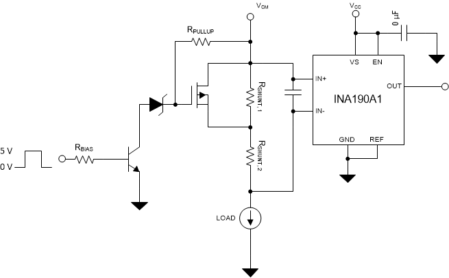 Figure 3-3 INA901 Schematic, 4 Decade
Measurement
Figure 3-3 INA901 Schematic, 4 Decade
MeasurementUtilization of such a topology does not come without its share of challenges. First, resistor choices must be made that do not cause undue harm to the load due to burden voltage of the chosen shunt resistors. Also, distortion effects may manifest during turn on and turn off times of the switch network, making the measurement unreliable during these transitions. Finally, as the FET must be controlled and keep track of which state it is in, logic is required for the use of such a topology. This is discussed in Section 4.
The design procedure is provided in the following steps:
- Bound the Upper Region: Begin by designing a shunt to the full output range of the chosen amplifier, taking power considerations into account. As calculated earlier, the maximum possible shunt for the upper region as designed in the previous section was 1.984 Ω. As it was determined that this level of dynamic range for a single device for the specified accuracy is unacceptable, the goal is then to create a second design for the lower portion of the design, and then stitch these two together via the turn on voltage of the FET. Therefore, select a point on the output curve that will serve as the transition point between the two regions. Ensure that the point selected continues to meet the desired specification with some margin. As observed in Total Output Error (%) Over Measurement Range, RSHUNT = 1.984 Ω, 100 µA to 100 mA, Ideal Shunt Tolerance, at 1 mA, the expected total error before shunt selection is < 2%, so this point is chosen as the cutoff point. As 1.984 Ω is not a standard resistor value, the closest standard value, rounding down, of 1.96 Ω is chosen.
- Design the Lower Region:
Using the lower bound of the upper region chosen in step 1, set this as the full scale input of the device, and
recalculate a second total shunt value for this region. Equation 7.This calculation shows, for this region, up to a 198.4-Ω shunt may be used. Selecting a value lower than 198.4-Ω is typically recommended. This value allows headroom for sizing, as well as hysteresis for more stable transition through both regions, if necessary. For convenience, 100 Ω is chosen here as the value of the lower range. Examining this value for the lower region, Total Output Error (%) Over Measurement Range, RSHUNT = 100 Ω, 10 µA to 1 mA, Ideal Shunt Tolerances presents the expected total output error for this resistance.
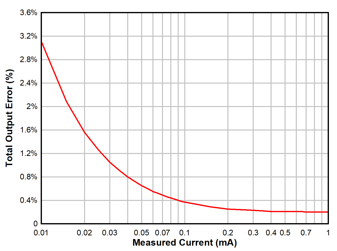 Figure 3-4 Total Output Error (%)
Over Measurement Range, RSHUNT = 100 Ω, 10 µA to 1 mA, Ideal
Shunt Tolerance
 - Choose the FET: Ideally, a
FET needs to be chosen with the smallest possible RDS(ON) available.
A challenge exists here in that typically, FETs with smaller RDS(ON)
values achieve this through larger substrates, so smaller values may be harder
to achieve for space-constrained applications. For this design, a CSD22206W
P-channel FET is chosen, with a maximum RDS(ON) of 5.7 mΩ (4.7 mΩ
typical) for
VGS = –4.5 V. - Confirm the Upper Shunt Value: For each of the design states, there is a combination of two elements that make up the shunt value of the design. When the FET is OFF, the elements are both RSHUNT, 1 and RSHUNT, 2 in series. As logic is used in such a design, the true nominal value may be programmed in logic, and the error is simply the worst-case tolerance values of the two resistors. As these resistors are in series and their values summed, provided the same tolerance value is chosen for both resistors, the worst-case tolerance error is simply the chosen tolerance value.
- Confirm the Lower Shunt
Value: When the FET is ON, the RDS(ON) becomes the dominant
contributing upper element, and the total shunt is this value in series with
RSHUNT, 2. Repeating the previous step for this region, it is
found that the nominal shunt value for the lower region is the sum of
RSHUNT, 2 and the typical RDS(ON) of the FET, or
1.9647 Ω. This is still less than the calculated maximum of 1.984 Ω, so is a
valid choice. While the tolerance of the RDS(ON) is large in
comparison to the resistance value of the FET, the overall contribution to the
total resistance value is small, and therefore does not cause excessive error,
as shown in Equation 8 and Equation 9. Equation 8.Equation 9.
- If Desired, Establish Hysteresis: If necessary, hysteretic set points may also be used to ensure stability of the FET transition point. The decision was made here to set hysteretic points at 1 mA and 1.5 mA to ensure smooth transition in the FET. This is discussed further in Control of the FET.
Output Voltage (V) Over Measurement Range, 10 µA to 100 mA shows the output range of the resulting design. Note that this curve shows the P-channel activation occurring at the 1.5 mA mark, in line with the previously-mentioned hysteretic forward point.
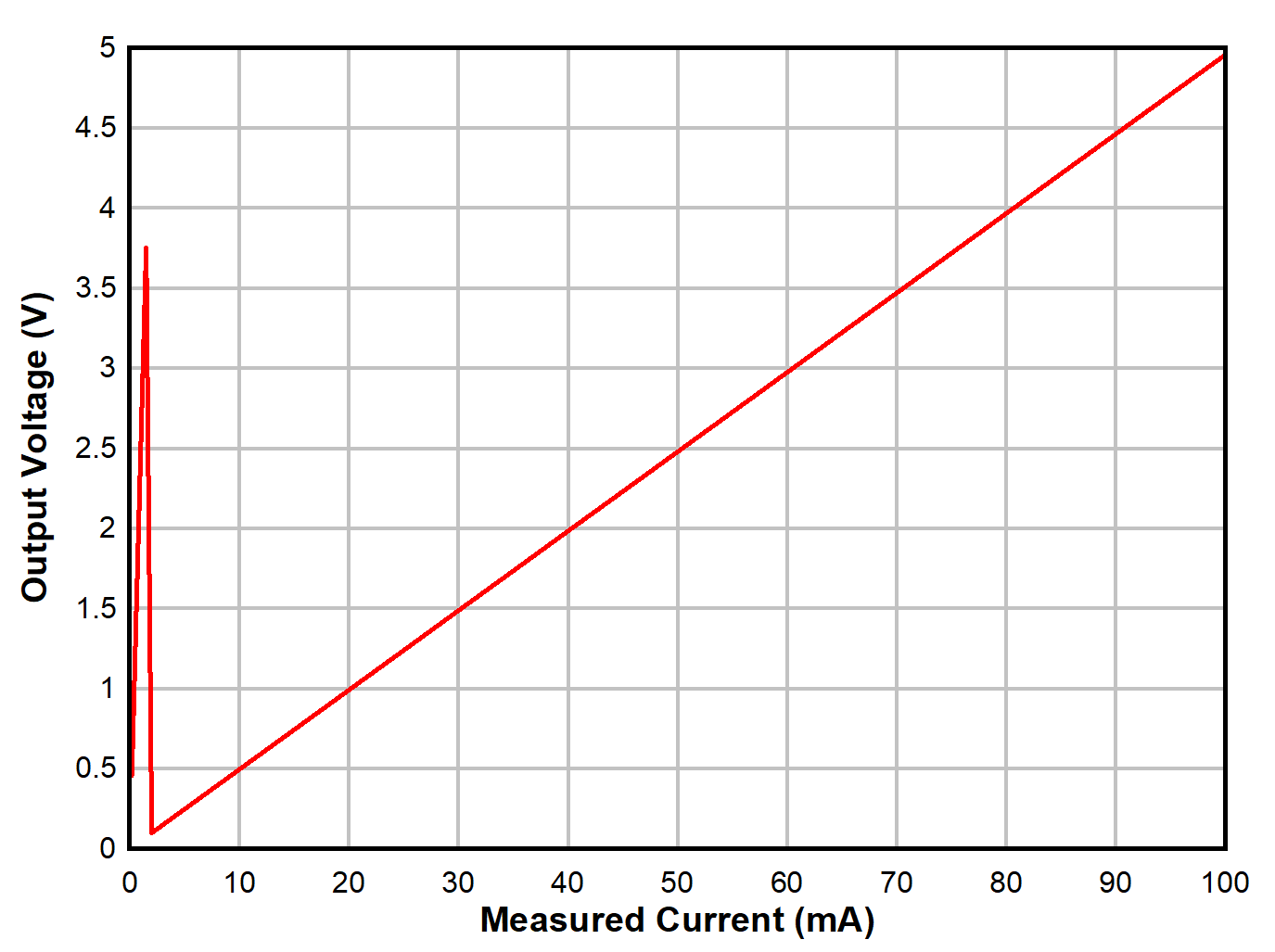 Figure 3-5 Output Voltage (V) Over
Measurement Range, 10 µA to 100 mA
Figure 3-5 Output Voltage (V) Over
Measurement Range, 10 µA to 100 mAOne important aspect to pay attention to is the actual decades of current measurement specified. While examining the full range of a current sense amplifier, it often may seem foolish to a new designer that such a small amount of the actual sensing range is dedicated to one of the sections designed, but Output Voltage (V) Over Measurement Range, 10 µA to 100 mA, Log Scale shows the same data as in Figure 3-5, with the x-axis now logarithmically based:
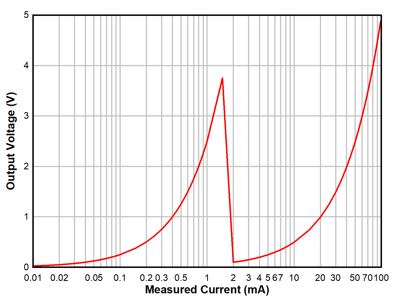 Figure 3-6 Output Voltage (V) Over
Measurement Range, 10 µA to 100 mA, Log Scale
Figure 3-6 Output Voltage (V) Over
Measurement Range, 10 µA to 100 mA, Log ScaleThe observation made viewing the range in log base is that each of these divisions occupies approximately the same proportional amount from a decades of measurement perspective, around 2 decades being handled per device. Various devices may be able to handle more or less by themselves, often dictated mainly by the worst-case offset voltage of the device.
The design was then simulated in TINA-TI to confirm the design expectations. INA190 Wide Measurement Schematic shows the simulation, along with measurement points.
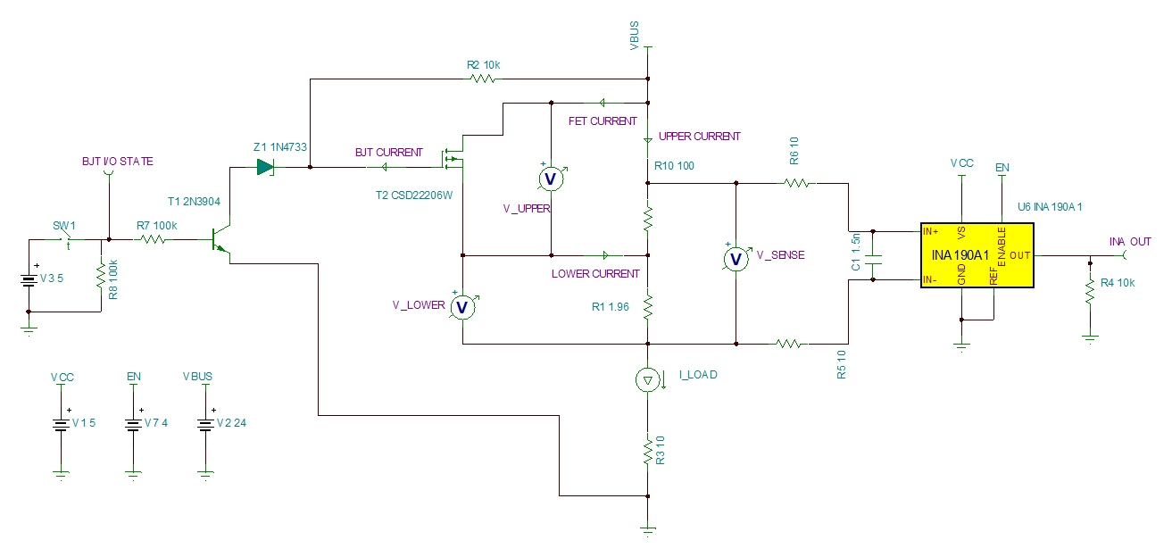 Figure 3-7 INA190 Wide Measurement
Schematic
Figure 3-7 INA190 Wide Measurement
SchematicFor the simulation, DC analysis was performed to examine expected outputs across the range. Table 3-1 lists the expected DC output for the circuit. Note that TINA-TI spice models contain typical parameters, so error at lower bounds is more in line with typical performance rather than worst case.
| Load Current | FET Status | Sense Voltage | INA Output Voltage, Actual | INA Output Voltage, Ideal(V) | Error (%) |
|---|---|---|---|---|---|
| 10 µA | OFF | 995.65 µV | 25.102 mV | 24.9 mV | 0.85 |
| 20 µA | OFF | 1.991 mV | 49.99 mV | 49.8 mV | 0.42 |
| 50 µA | OFF | 4.978 mV | 124.656 mV | 124 mV | 0.17 |
| 75 µA | OFF | 7.467 mV | 186.876 mV | 187 mV | 0.11 |
| 100 µA | OFF | 9.956 mV | 249.1 mV | 249 mV | 0.08 |
| 200 µA | OFF | 19.912 mV | 497.98mV | 498 mV | 0.04 |
| 500 µA | OFF | 49.779 mV | 1.245 V | 1.24 V | 0.01 |
| 750 µA | OFF | 74.669 mV | 1.867 V | 1.87 V | 0.01 |
| 1 mA | OFF | 99.558 mV | 2.489 V | 2.49 V | 0.01 |
| 2 mA | ON | 3.943 mV | 98.790 mV | 98.6 mV | 0.21 |
| 5 mA | ON | 9.837 mV | 246.118 mV | 246 mV | 0.08 |
| 7.5 mA | ON | 14.748 mV | 368.890 mV | 369 mV | 0.05 |
| 10 mA | ON | 19.66 mV | 491.663 mV | 491 mV | 0.04 |
| 20 mA | ON | 39.304 mV | 982.753 mV | 983 mV | 0.02 |
| 50 mA | ON | 98.238 mV | 2.456 V | 2.46 V | 0.01 |
| 75 mA | ON | 147.35 mV | 3.684 V | 3.68 V | 0.01 |
| 100 mA | ON | 196.461 mV | 4.911 V | 4.91 V | 0.01 |
For AC response, a time-based step response signal was utilized along with a time-based switch to mimic the transition of the GPIO pin controlling the gate. In implementation, this logic transition is performed via GPIO, using the digitized output as a feedback to keep track in logic, and would also exhibit some amount of delay. Note that as shown in Step Response (10-mVPP Input Step) of the INA190 Bidirectional, Low-Power, Zero-Drift, Wide Dynamic Range, Precision Current-Sense Amplifier With Enable data sheet, approximately 40 µs is needed for the INA190 output to settle to steady state. INA190 4-Decade Design Dynamic Response exhibits the values required for the INA190 output to settle to steady state.
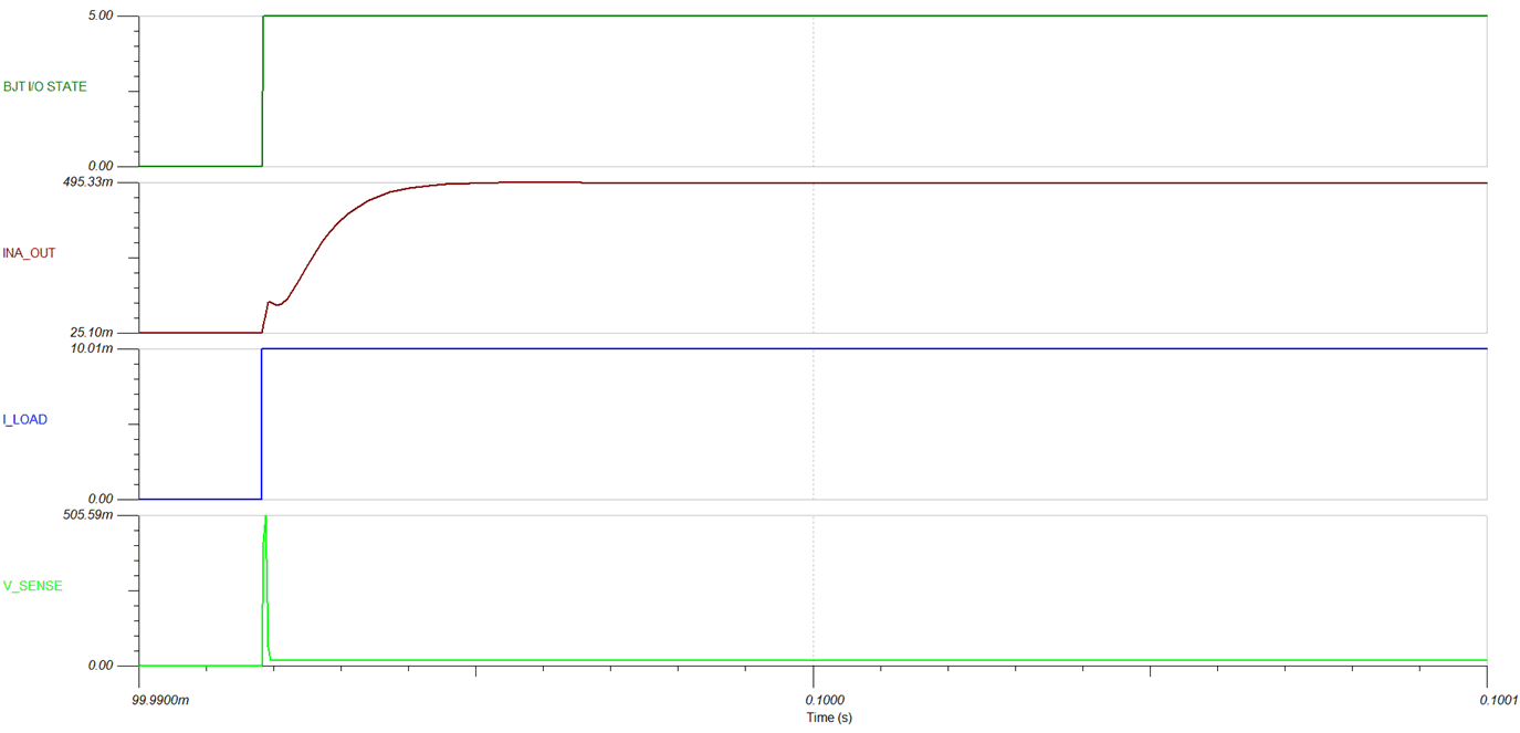 Figure 3-8 INA190 4-Decade Design Dynamic
Response
Figure 3-8 INA190 4-Decade Design Dynamic
ResponseAs expected, observe that there is some amount of distortion as the FET activates and changes the effective resistance between states.