SBOS469H April   2009  – October 2023 INA199

PRODUCTION DATA  

  1.   1
  2. Features
  3. Applications
  4. Description
  5. Device Comparison Table
  6. Pin Configuration and Functions
  7. Specifications
    1. 6.1 Absolute Maximum Ratings
    2. 6.2 ESD Ratings
    3. 6.3 Recommended Operating Conditions
    4. 6.4 Thermal Information
    5. 6.5 Electrical Characteristics
    6. 6.6 Typical Characteristics
  8. Detailed Description
    1. 7.1 Overview
    2. 7.2 Functional Block Diagram
    3. 7.3 Feature Description
      1. 7.3.1 Basic Connections
      2. 7.3.2 Selecting RS
    4. 7.4 Device Functional Modes
      1. 7.4.1 Input Filtering
      2. 7.4.2 Shutting Down the INA199 Series
      3. 7.4.3 REF Input Impedance Effects
      4. 7.4.4 Using the INA199 With Common-Mode Transients Above 26 V
      5. 7.4.5 Improving Transient Robustness
  9. Application and Implementation
    1. 8.1 Application Information
    2. 8.2 Typical Applications
      1. 8.2.1 Unidirectional Operation
        1. 8.2.1.1 Design Requirements
        2. 8.2.1.2 Detailed Design Procedure
        3. 8.2.1.3 Application Curve
      2. 8.2.2 Bidirectional Operation
        1. 8.2.2.1 Design Requirements
        2. 8.2.2.2 Detailed Design Procedure
        3. 8.2.2.3 Application Curve
  10. Power Supply Recommendations
  11. 10Layout
    1. 10.1 Layout Guidelines
    2. 10.2 Layout Example
  12. 11Device and Documentation Support
    1. 11.1 Documentation Support
      1. 11.1.1 Related Documentation
    2. 11.2 Receiving Notification of Documentation Updates
    3. 11.3 Support Resources
    4. 11.4 Trademarks
    5. 11.5 Electrostatic Discharge Caution
    6. 11.6 Glossary
  13. 12Revision History
  14. 13Mechanical, Packaging, and Orderable Information

Description

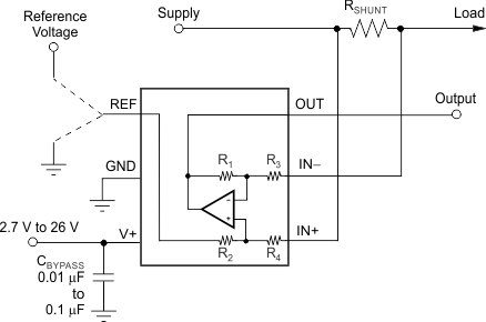
The INA199 series of voltage-output, current-shunt monitors (also called current-sense amplifiers) are commonly used for overcurrent protection, precision-current measurement for system optimization, or in closed-loop feedback circuits. This series of devices can sense drops across shunt resistors at common-mode voltages from –0.3 V to 26 V, independent of the supply voltage. Three fixed gains are available: 50 V/V, 100 V/V, and 200 V/V. The low offset of the zero-drift architecture enables current sensing with maximum drops across the shunt as low as 10-mV full-scale.

These devices operate from a single 2.7-V to 26-V power supply, drawing a maximum of 100 µA of supply current. All versions are specified from –40°C to 125°C, and offered in both SC70-6 and thin UQFN-10 packages.

Device Information
PART NUMBER PACKAGE(1) BODY SIZE (NOM)
INA199 SC70 (6) 2.00 mm × 1.25 mm
UQFN (10) 1.80 mm × 1.40 mm
For all available packages, see the orderable addendum at the end of the data sheet.
GUID-54CBB9E0-9F67-4E23-B22F-6A7FD4E02D15-low.gif Simplified Schematic