SBOSA02A August   2021  – April 2025 OPA2397 , OPA397 , OPA4397

PRODMIX  

  1.   1
  2. Features
  3. Applications
  4. Description
  5. Pin Configuration and Functions
  6. Specifications
    1. 5.1 Absolute Maximum Ratings
    2. 5.2 ESD Ratings
    3. 5.3 Recommended Operating Conditions
    4. 5.4 Thermal Information OPA397
    5. 5.5 Thermal Information OPA2397
    6. 5.6 Thermal Information OPA4397
    7. 5.7 Electrical Characteristics
    8. 5.8 Typical Characteristics
  7. Detailed Description
    1. 6.1 Overview
    2. 6.2 Functional Block Diagram
    3. 6.3 Feature Description
      1. 6.3.1 Low Operating Voltage
      2. 6.3.2 Low Input Bias Current
    4. 6.4 Device Functional Modes
  8. Application and Implementation
    1. 7.1 Application Information
    2. 7.2 Typical Application
      1. 7.2.1 Design Requirements
      2. 7.2.2 Detailed Design Procedure
      3. 7.2.3 Application Curve
    3. 7.3 Power Supply Recommendations
    4. 7.4 Layout
      1. 7.4.1 Layout Guidelines
      2. 7.4.2 Layout Example
  9. Device and Documentation Support
    1. 8.1 Device Support
      1. 8.1.1 Development Support
        1. 8.1.1.1 TINA-TI™ Simulation Software (Free Download)
    2. 8.2 Documentation Support
      1. 8.2.1 Related Documentation
    3. 8.3 Receiving Notification of Documentation Updates
    4. 8.4 Support Resources
    5. 8.5 Trademarks
    6. 8.6 Electrostatic Discharge Caution
    7. 8.7 Glossary
  10. Revision History
  11. 10Mechanical, Packaging, and Orderable Information

Low Input Bias Current

The typical input bias current of the OPAx397 is extremely low (typically 10fA). Input bias current is dominated by leakage current from the ESD protection diodes, which is proportional to the area of the diode. The OPAx397 is able to achieve ultra-low input bias current as a result of modern process technology and advanced electrostatic discharge (ESD) protection design that minimizes the area of the diode.

In overdriven conditions, the bias current can increase significantly. The most common cause of an overdriven condition occurs when the operational amplifier is outside of the linear range of operation. When the output of the operational amplifier is driven to one of the supply rails, the feedback loop requirements cannot be satisfied and a differential input voltage develops across the input pins. This differential input voltage results in the forward-biasing of the ESD cells. Figure 6-1 shows the equivalent circuit.
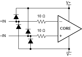
OPA397 OPA2397 OPA4397 Equivalent Input Circuit Figure 6-1 Equivalent Input Circuit