SBOU231 October 2020 OPA3S328
7.2 PCB Layout
The OPA3S328EVM is a four-layer PCB design. Figure 7-3 to Figure 7-7 show the PCB layer illustrations. The top layer consists of all signal path traces, and is poured with a solid ground plane. Site 1 decoupling supply capacitors C7, C9, C10, and C11 are positioned on the top layer as close as possible to the power supply pins of device U1. Similarly, site 2 decoupling supply capacitors C17, C19, C20, and C21 are placed as close as possible to the power supply pins of the device U2. Selectable gain resistors and compensation capacitors are placed in close proximity to the inverting terminal of the corresponding operational amplifier forming a small feedback loop. The second internal layer is a dedicated solid GND plane. Independent vias to ground are placed at the ground connection of every component to provide a low-impedance, short path to ground. The third internal layer routes the power-supply connections. The bottom layer routes additional signal traces and the switch control signals.
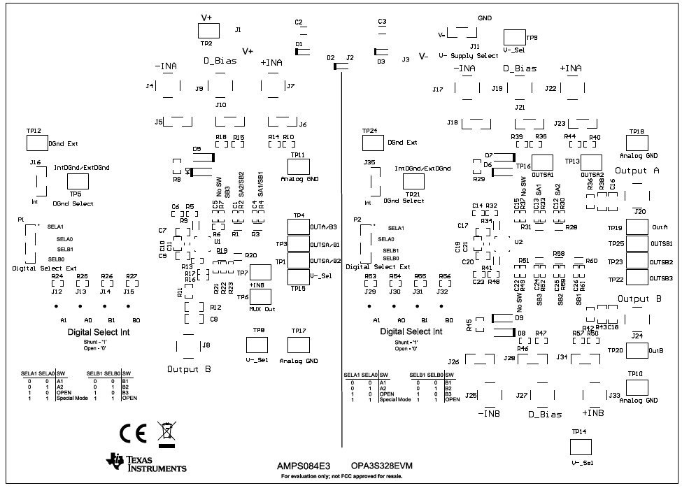 Figure 7-3 Top Overlay.
 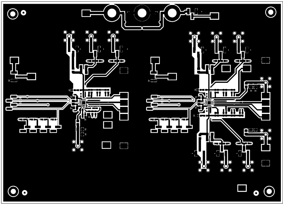 Figure 7-4 Top Layer
PCB Layout
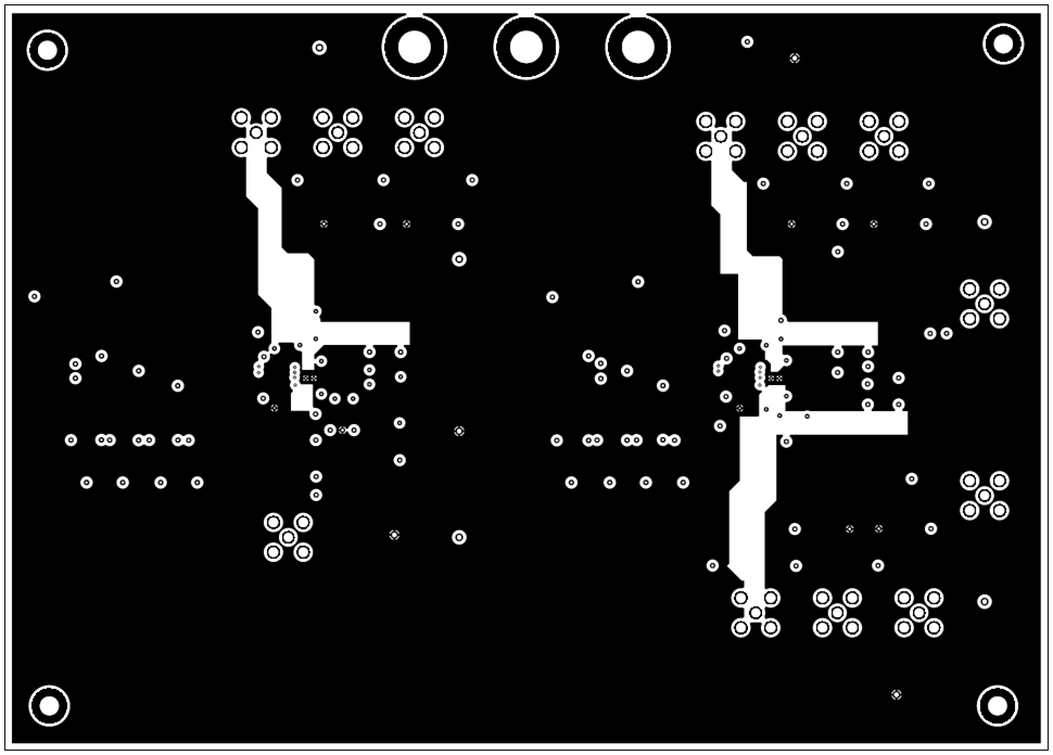 Figure 7-5 Ground
Layer PCB Layout
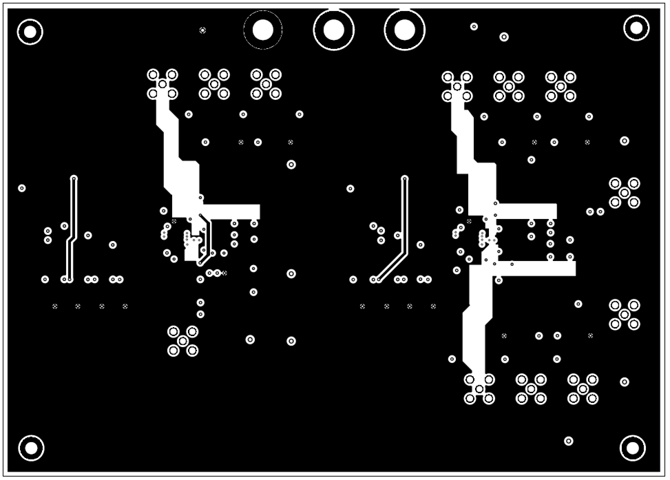 Figure 7-6 Power
Layer PCB Layout
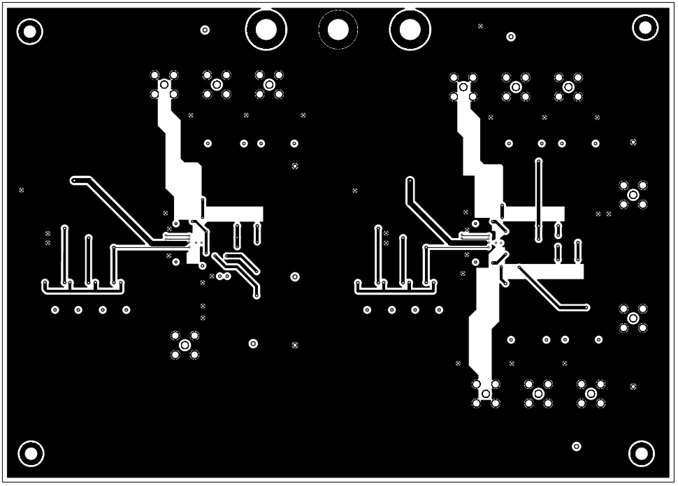 Figure 7-7 Bottom
Layer PCB Layout