SBOU254A January 2021 – June 2021
5.1 Schematics
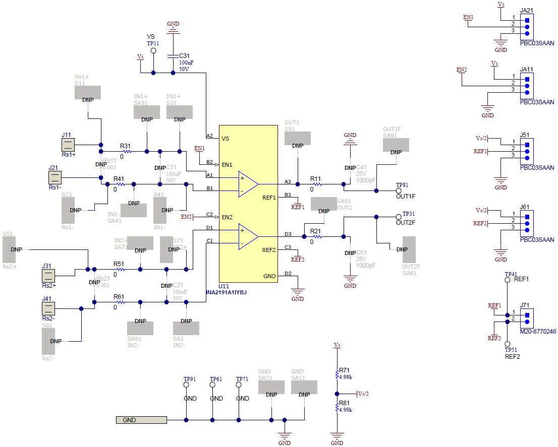
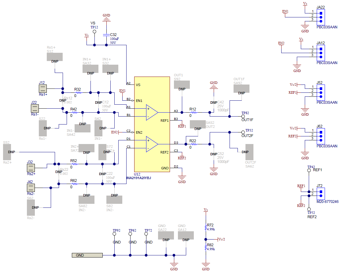
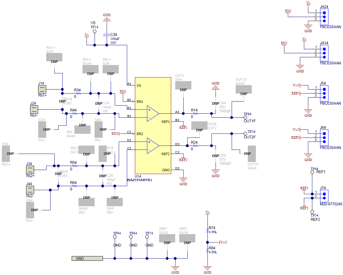
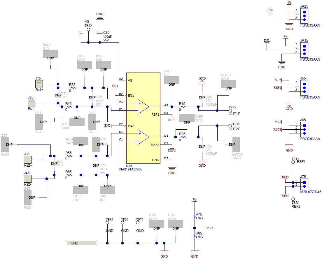
Figure 5-1 through Figure 5-5 show the schematics for the A pinout of the INA2191EVM PCB for all gain options.
 Figure 5-1 INA2191EVM Schematic: Gain A1
Panel
 Figure 5-2 INA2191EVM Schematic: Gain A2
Panel
 Figure 5-3 INA2191EVM Schematic: Gain A3
Panel
 Figure 5-4 INA2191EVM Schematic: Gain A4
Panel
 Figure 5-5 INA2191EVM Schematic: Gain A5
Panel