SBVS080J September 2006 – November 2016 TPS75100 , TPS75103 , TPS75105
PRODUCTION DATA.
- 1 Features
- 2 Applications
- 3 Description
- 4 Revision History
- 5 Pin Configuration and Functions
- 6 Specifications
- 7 Detailed Description
- 8 Application and Implementation
- 9 Power Supply Recommendations
- 10Layout
- 11Device and Documentation Support
- 12Mechanical, Packaging, and Orderable Information
8 Application and Implementation
NOTE
Information in the following applications sections is not part of the TI component specification, and TI does not warrant its accuracy or completeness. TI’s customers are responsible for determining suitability of components for their purposes. Customers should validate and test their design implementation to confirm system functionality.
8.1 Application Information
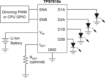
The TPS7510x provides a constant current to up to four unmatched LEDs organized in two banks of two LEDs each in a common-cathode topology. Without an external resistor, the current source defaults to a factory-programmable, preset current level with ±0.5% accuracy (typical). An optional external resistor can be used to set initial brightness to user-programmable values with higher accuracy. Brightness can be varied from off to full brightness by inputting a pulse width modulation (PWM) signal on each enable pin (ENx, where x indicates LED bank A or B). Each bank has independent enable and brightness control, but current matching is done to all four channels concurrently. The input supply range is ideally suited for single-cell Li-Ion battery supplies and the TPS7510x can provide up to 25 mA per LED. No internal switching signals are used, eliminating troublesome electromagnetic interference (EMI). The device is fully specified over TJ = –40°C to +85°C.
8.1.1 Setting the Output Current Level
The TPS7510x is a quad matched current source. Each of the four current source output levels is set by a single reference current. An internal voltage reference of 1.225 V (nominal) in combination with a resistor sets the reference current level. This reference current is then mirrored onto each of the four outputs with a ratio of typically 420:1. The resistor required to set the LED current is calculated using Equation 1:

where
- K is the current ratio
- VISET is the internal reference voltage
- ILED is the desired LED current
For example, to set the LED current level to 10mA, a resistor value of 51.1 kΩ is required. This value sets up a reference current of 23.9 μA (1.22 V / 51.1 kΩ). In turn, this reference current is mirrored to each output current source, resulting in an output current of 10 mA (23.9 μA × 420).
The TPS7510x offers two methods for setting the output current levels. The LED current is set either by connecting a resistor (calculated using Equation 1) from the ISET pin to GND, or leaving ISET unconnected to employ the factory-programmed RSET resistance. The internal programmed resistance is implemented using high-precision processing and yields a reference current accuracy of 0.5%, nominal. Accuracy using external resistors is subject to the tolerance of the external resistor and the accuracy of the internal reference voltage.
The TPS7510x automatically detects the presence of an external resistor by monitoring the current out of the ISET pin. Current levels in excess of 3 μA signify the presence of an external resistor and the device uses the external resistor to set the reference current. If the current from ISET is less than 3 μA, the device defaults to the preset internal reference set resistor. The TPS7510x is available with eight preset current levels, from 3 mA to 10 mA (per output) in 1-mA increments. Solutions using the preset internal current level eliminate an external component, thereby increasing accuracy and reducing cost.
Table 1. Recommended (1% Tolerance) Set Resistor Values
| RSET (kΩ) | ISET (μA) | IDX (mA)(1) |
|---|---|---|
| 511 | 2.4 | 1.0 |
| 255 | 4.8 | 2.0 |
| 169 | 7.2 | 3.0 |
| 127 | 9.6 | 4.1 |
| 102 | 12.0 | 5.0 |
| 84.5 | 14.5 | 6.1 |
| 73.2 | 16.7 | 7.0 |
| 64.9 | 18.9 | 7.9 |
| 56.2 | 21.8 | 9.2 |
| 51.1 | 24.0 | 10.1 |
| 46.4 | 26.4 | 11.1 |
| 42.2 | 29.0 | 12.2 |
| 39.2 | 31.3 | 13.1 |
| 36.5 | 33.6 | 14.1 |
| 34.0 | 36.0 | 15.1 |
| 32.4 | 37.8 | 15.9 |
| 30.1 | 40.7 | 17.1 |
| 28.7 | 42.7 | 17.9 |
| 26.7 | 45.9 | 19.3 |
| 25.5 | 48.0 | 20.2 |
| 24.3 | 50.4 | 21.2 |
| 23.2 | 52.8 | 22.2 |
| 22.1 | 55.4 | 23.3 |
| 21.5 | 57.0 | 23.9 |
| 20.5 | 59.8 | 25.1 |
8.1.2 Limitations on LED Forward Voltages
The TPS7510x is a linear current source implementing LDO regulator building blocks. Therefore, to maintain accurate operation, there are some limitations to the forward (output) voltages that can be used. The first limitation is the maximum LED forward voltage. The dropout voltage must be considered because LDO technology is employed. The TPS7510x is an ultra-low dropout device with typical dropouts in the range of 30 mV at 5 mA. Care must be taken in the design to ensure that the difference between the lowest possible input voltage (for example, battery cut-off) and the highest possible forward voltage yields at least 100 mV of headroom. Headroom levels less than dropout decrease the accuracy of the current source (see Figure 6).
The other limitation to consider is the minimum output voltage required to yield accurate operation. The current source employs NMOS MOSFETs, and a minimum forward LED voltage of approximately 1.5 V on the output is required to maintain highest accuracy. The TPS7510x is ideal for white LEDs and color LEDs with forward voltages greater than 1.5 V. This range includes red LEDs that have typical forward voltages of 1.7 V.
8.1.3 Use of External Capacitors
The TPS7510x does not require the use of any external capacitors for stable operation. Nominal stray and power-supply decoupling capacitance on the input is adequate for stable operation. Capacitors are not needed for stability and are therefore not recommended on the outputs.
8.1.4 Use of Unused Outputs or Tying Outputs Together
Unused outputs can be left unconnected or tied to the VIN supply. Although open outputs are acceptable, tying unused outputs to the VIN supply increases ESD protection. Connecting unused outputs to ground violates the minimum recommended output voltage, results in current levels that potentially exceed the set or preset LED current, and must be avoided.
Connecting outputs in parallel is an acceptable way of increasing the amount of LED current drive. This configuration is a useful trick when the higher current level is a multiple of the preset value.
8.1.5 Use of Enable Pins for PWM Dimming
The TPS7510x divides control of the LED outputs into two banks of two current sources each. Each bank is controlled by the use of an independent, active-high enable pin (ENA and ENB). The enable pin can be used for standard ON or OFF operation of the current source, driven by standard logic levels from processor GPIO pins, for example. Drive ENx high to turn on the bank of LEDs; drive ENx low to turn off the bank of LEDs.
Another use of the enable pins is for LED dimming. LED brightness is a function of the current level being driven across the diode and the time that current is being driven through the diode. The perceived brightness of an LED can be changed by either varying the current level or, more effectively, by changing the time in which that current is present. When a PWM signal is input into the enable pin, the duty cycle (high- or on-time) determines how long the fixed current is driven across the LEDs. Reducing or increasing that duration has the effect of dimming or brightening the LED, without having to employ the more complex method of varying the current level. This technique is particularly useful for reducing LED brightness in low ambient light conditions, where LED brightness is not required, thereby decreasing current consumption. The enable pins can also be used for LED blinking, varying blink rates based on system status.
Although providing many useful applications, PWM dimming does have a minimum duty cycle required to achieve the required current level. The recommended minimum on-time of the TPS7510x is approximately 33 μs. On-times less than 33 μs result in reductions in the output current by not allowing enough time for the output to reach the desired current level. Also, having both enables switching together, asynchronously, or having one enable on at all times, effects the minimum recommended on-time (see Figure 4 and Figure 5). If one enable is already on, the speed at which the other channel turns on is faster than if both channels are turning on together or if the other channel is off. Therefore, already having one channel enabled allows for approximately 10-μs to 12-μs shorter minimum on-times for the switching channel.
Unused enable pins can be left unconnected or connected to ground to minimize current consumption. Connecting unused enable pins to ground increases ESD protection. If connected to VIN, a small amount of current drains through the enable input (see the Electrical Characteristics table).
8.2 Typical Application
8.2.1 Design Requirements
Table 2 shows the design requirements.
Table 2. Design Parameters
| PARAMETER | DESIGN REQUIREMENT |
|---|---|
| Input voltage | 3.8 V |
| Number of LEDs | 4 |
| LED current | 5 mA (per LED) |
8.2.2 Detailed Design Procedure
Select the TPS75105 so that no external resistor is required to set the LED current.
8.2.3 Application Curve

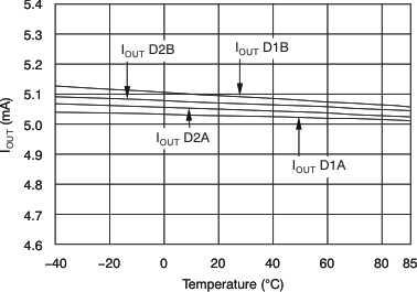
| RSET = open |
