SCEU022A September 2020 – September 2022
2.1 PCB Overview
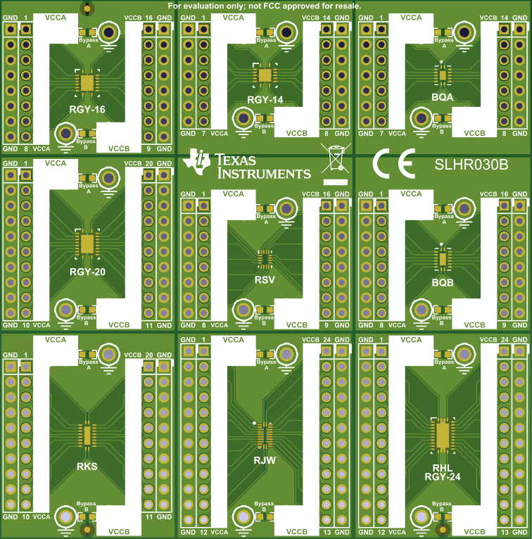
Figure 2-1 shows the EVM PCB.
 Figure 2-1 14-24-NL-Logic-EVM PCB
The 14-24-NL-Logic-EVM PCB is designed to be straightforward for new users to begin evaluating NL logic and translation devices. This section highlights a few aspects of the PCB, which are as follows:
- Board is breakable into smaller sections with the inclusion of v-scored grooves
- Each section has headers connected to device pins, VCCA, VCCB, and GND
- Designated supply inputs with included thru-hole test points
- Bypass capacitor footprints included for device supplies (capacitors not included in kit)
- Option for single supply or dual supply evaluation with easy configuration