SFFS032 December 2022 TLV6001-Q1 , TLV6002-Q1
4.1 SC70 Package
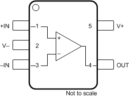
Figure 4-1 shows the TLV600x-Q1 pin diagram for the SC70 package. For a detailed description of the device pins please refer to the Pin Configuration and Functions section in the TLV600x-Q1 data sheet.
 Figure 4-1 Pin Diagram (SC70) Package
| Pin Name | Pin No. | Description of Potential Failure Effect(s) | Failure Effect Class |
|---|---|---|---|
| +IN | 1 |
Input at V- is valid input; however desired application result is unlikely. Output will be low, if other input is greater than V- potential. |
C |
|
V- |
2 |
Normal operation, unless dual supply voltage was intended. |
D |
|
-IN |
3 | Input at V- is valid input; however desired application result is unlikely. Output will be high, if other input is greater than V- potential. |
C |
|
OUT |
4 |
May cause device to overheat due to output short circuit current. |
B |
|
V+ |
5 | Diodes from input to V+ may turn on due to input signal and cause EOS. | B |
| Pin Name | Pin No. | Description of Potential Failure Effect(s) | Failure Effect Class |
|---|---|---|---|
| +IN | 1 | Floating input, circuit will likely not function as expected. | C |
|
V- |
2 | Lowest voltage pin will try to power internal ground via ESD diode to V- pin. | B |
|
-IN |
3 | Floating input, circuit will likely not function as expected. |
C |
|
OUT |
4 | Output can't be used by application. |
C |
|
V+ |
5 | Highest voltage pin will try to power internal ground via ESD diode to V+. | B |
| Pin Name | Pin No. | Shorted to | Description of Potential Failure Effect(s) | Failure Effect Class |
|---|---|---|---|---|
|
+IN |
1 |
V- |
Input at V- is valid input, however, desired application result is unlikely. | C |
| V- | 2 |
-IN |
Input at V- is valid input, however, desired application result is unlikely. | C |
| -IN | 3 | OUT | Negative feedback, creates unity gain buffer. | C |
| OUT | 4 | V+ | May cause overheating, as the output tries to sink current from V+. | B |
| V+ | 5 | +IN | Input at V+ is valid input, however, desired application result is unlikely. | C |
| Pin Name | Pin No. | Description of Potential Failure Effect(s) | Failure Effect Class |
|---|---|---|---|
| +IN | 1 | Input at V+ is valid input; however desired application result is unlikely. Output will be high, if -IN is lower than V+ potential. | C |
|
V- |
2 | Diodes from V- to V+ may turn on due to input signal and cause EOS. | B |
|
-IN |
3 | Input at V+ is valid input; however desired application result is unlikely. Output will be low, if +IN is lower than V+ potential. |
C |
|
OUT |
4 | May cause overheating, as the output tries to sink current from V+. |
C |
|
V+ |
5 | Normal operation | B |