SFFS172 August 2021 REF20-Q1
4 Pin Failure Mode Analysis (Pin FMA)
This section provides a Failure Mode Analysis (FMA) for the pins of the REF20-Q1. The failure modes covered in this document include the typical pin-by-pin failure scenarios:
- Pin short-circuited to Ground (see Table 4-2)
- Pin open-circuited (see Table 4-3)
- Pin short-circuited to an adjacent pin (see Table 4-4)
- Pin short-circuited to supply (see Table 4-5)
Table 4-2 through Table 4-5 also indicate how these pin conditions can affect the device as per the failure effects classification in Table 4-1.
| CLASS | FAILURE EFFECTS |
|---|---|
| A | Potential device damage that affects functionality |
| B | No device damage, but loss of functionality |
| C | No device damage, but performance degradation |
| D | No device damage, no impact to functionality or performance |
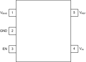
Figure 4-1 shows the REF20-Q1 pin diagram. For a detailed description of the device pins please refer to the Pin Configuration and Functions section in the REF20-Q1data sheet.
 Figure 4-1 Pin Diagram
Unless otherwise specified, it is assumed that the voltages applied to all the pins are within the Recommended Operating Range specified in the datasheet.
| PIN NAME | PIN NO. | DESCRIPTION OF POTENTIAL FAILURE EFFECT(S) | FAILURE EFFECT CLASS |
|---|---|---|---|
| VBIAS | 1 | Might damage the device, can affect functionality. Forces short circuit current to flow through device. | A |
| GND | 2 | Normal operation. | D |
| EN | 3 | No device damage. Device output will be disabled. System current may increase. | B |
| VIN | 4 | No device damage. Device will not generate output. Increased system current. | B |
| VREF | 5 | Might damage the device, can affect functionality. Forces short circuit current to flow through device. | A |
| PIN NAME | PIN NO. | DESCRIPTION OF POTENTIAL FAILURE EFFECT(S) | FAILURE EFFECT CLASS |
|---|---|---|---|
| VBIAS | 1 | No bias output voltage. | B |
| GND | 2 | No output voltage. | B |
| EN | 3 | No damage to device, can affect functionality. | B |
| VIN | 4 | Device is unpowered. | B |
| VREF | 5 | No reference output voltage. | B |
| PIN NAME | PIN NO. | SHORTED TO | DESCRIPTION OF POTENTIAL FAILURE EFFECT(S) | FAILURE EFFECT CLASS |
|---|---|---|---|---|
| VBIAS | 1 | GND | Might damage the device, can affect functionality. Forces short circuit current to flow through device. | A |
| GND | 2 | EN | No device damage. Device output will be disabled. | B |
| EN | 3 | VIN | No damage to device. Device disable functionality will be lost. System current may increase. | B |
| VIN | 4 | VREF | Might damage the device. High current flow into the reference output. | A |
| VREF | 5 | VBIAS | Might damage the device. High current will flow from reference output to bias output. | A |
| PIN NAME | PIN NO. | DESCRIPTION OF POTENTIAL FAILURE EFFECT(S) | FAILURE EFFECT CLASS |
|---|---|---|---|
| VBIAS | 1 | Might damage the device. High current flow into the bias output. | A |
| GND | 2 | No device damage. Device will not generate output. Increased system current. | B |
| EN | 3 | No damage to device. Device disable functionality will be lost. System current may increase. | B |
| VIN | 4 | Normal operation. | D |
| VREF | 5 | Might damage the device. High current flow into the bias output. | A |