SFFS311 October 2021 LMR51420 , LMR51430
4 Pin Failure Mode Analysis (Pin FMA)
This section provides a Failure Mode Analysis (FMA) for the pins of the LMR51420 and LMR51430. The failure modes covered in this document include the typical pin-by-pin failure scenarios:
- Pin short-circuited to Ground (see Table 4-2)
- Pin open-circuited (see Table 4-3)
- Pin short-circuited to an adjacent pin (see Table 4-4)
- Pin short-circuited to supply (see Table 4-5)
Table 4-2 through Table 4-5 also indicate how these pin conditions can affect the device as per the failure effects classification in Table 4-1.
| Class | Failure Effects |
|---|---|
| A | Potential device damage that affects functionality |
| B | No device damage, but loss of functionality |
| C | No device damage, but performance degradation |
| D | No device damage, no impact to functionality or performance |
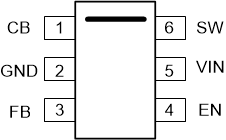
Figure 4-1 shows the LMR51420 and LMR51430 pin diagram. For a detailed description of the device pins please refer to the 'Pin Configuration and Functions' section in the LMR51420 and LMR51430 datasheet.
 Figure 4-1 Pin Diagram
Following are the assumptions of use and the device configuration assumed for the pin FMA in this section:
- Application circuit, as per the LMR51430 data sheet is used.
| Pin Name | Pin No | Description of Potential Failure Effect(s) | Failure Effect Class |
|---|---|---|---|
| GND | 1 | Normal operation | D |
| SW | 2 | Damage to HS FET | A |
| VIN | 3 | VOUT = 0 V | B |
| FB | 4 | VOUT >> than programmed output voltage | B |
| EN | 5 | VOUT = 0 V | B |
| CB | 6 | VOUT = 0 V | B |
| Pin Name | Pin No | Description of Potential Failure Effect(s) | Failure Effect Class |
|---|---|---|---|
| GND | 1 | VOUT can be abnormal due to switching noise on analog circuits. | B |
| SW | 2 | VOUT = 0 V | B |
| VIN | 3 | Device can shut off | B |
| FB | 4 | VOUT >> than programmed output voltage | B |
| EN | 5 | Device can shut off | B |
| CB | 6 | VOUT = 0 V | B |
| Pin Name | Pin No | Description of Potential Failure Effect(s) | Failure Effect Class |
|---|---|---|---|
| GND | SW | Damage to HS FET | A |
| SW | VIN | Damage to LS FET | A |
| CB | EN | EN pin ESD Damage if VIN > 31 V | A |
| EN | FB | EN voltage lower than 5.5 V, VOUT = 0 V | B |
| EN higher than 5.5 V, damage to FB | A |
| Pin Name | Pin No | Description of Potential Failure Effect(s) | Failure Effect Class |
|---|---|---|---|
| GND | 1 | VOUT = 0 V. Damage to other pins referred to GND | A |
| SW | 2 | Damage to LS FET | A |
| VIN | 3 | Normal mode | D |
| FB | 4 |
If VIN exceeds 5.5 V damage will occur, VOUT = 0 V. |
A |
| EN | 5 | Device enabled | D |
| CB | 6 | VOUT = 0 V. CBOOT ESD clamp will run current to destruction. | A |