SLAAE18 March 2021 MSP430FR2433
1 Application Brief
Introduction
Many applications, such as toys, musical tuners, function generators, and others require the generation of reference analog waveforms and signals. Although this can be done with a digital-to-analog converter (DAC), this can also be achieved with a few passive components and a pulse width modulated (PWM) signal. This document demonstrates how to generate time-variant and static signals; however, it can be adapted to construct many other arbitrary signals using tables or counters, multiple programmable DAC levels, or a combination. This example demonstrates an 8-bit DAC generating a 250Hz sine wave, oversampled at 16x, and a DC signal without GUI visualization and a 4Hz sine wave, oversampled at 16x, and a DC signal with analog-to-digital converter (ADC) capture and GUI visualization. The sine wave is achieved by storing the sine samples in a lookup table and updating the PWM duty cycle duration with the next sample after each PWM cycle. The PWM is output to an RC filter that removes the higher-frequency signal components and reconstructs the sine wave. For this reason, it is best for the PWM frequency to be much higher than the desired sine frequency. To generate the static signal, a constant duty cycle is maintained. The MSP430FR2433 MCU, which is used in this document, is a cost-effective device with 4KB of SRAM and 16KB of FRAM.
Implementation
In Figure 1-1, the sine PWM duty cycle is changing after each PWM period, whereas, the DC duty cycle is not. The sine and DC waves are seen at the output of the RC filters.
 Figure 1-1 PWMs and Output
The resolution of the DAC is determined by the timer count length (28 = 256). The sampling rate, or PWM frequency, can be found by multiplying the sine frequency by the number of samples per sine cycle, which gives 8 kHz.
An easy way to think about this relationship is that the capacitor is essentially averaging the output samples over time. The sampling rate is the output sample speed required to construct a 250Hz periodic signal with 32 samples per cycle. The PWM clock frequency is found by multiplying the sampling frequency by the number of timer counts, which gives 2.048 MHz. To achieve this, the digitally controlled oscillator (DCO) has been set to 16 MHz with a subsystem master clock (SMCLK) divider of 8. The relationship between resolution, PWM frequency, and PWM clock frequency is shown in Equation 2.
where, nBits = the bit resolution of the DAC.
The CCR0 interrupt is enabled and the ISR updates the PWM duty cycle stored in CCR1. This is done by incrementing the counter variable to point within a 32-element sine wave array. CCR2 is loaded with a constant PWM duty cycle to generate the DC signal. CCR1 and CCR2 are configured for pins P1.1/TA0.1 and P1.2/TA0.2. Both CCR output modes are set to reset/set. In this mode, each output is reset when the counter reaches the respective CCRx value and is set when the counter reaches the CCR0 value. This provides positive pulses equivalent to the value in CCRx on each respective output.
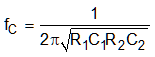
By outputting the sine PWM to a 2-pole RC filter, the sine wave is reconstructed and the PWM switching is filtered out. The R and C values can be determined by Equation 3, where R1C1 = R2C2 = RC:

The filter cutoff (795Hz) is chosen to be sufficiently higher than the bandwidth edge to reduce attenuation, and lower than the frequency of the PWM signal to filter out its switching. This filter gives better response when R2>>R1, due to the effect of the voltage divider that is present. The second order passive filter topology was chosen for its simplicity. The filter for the DC signal is simply used for charge storage; thus, a single-pole filter is implemented. This solution uses an MSP430FR2433 MCU and external resistors and capacitors to build the RC filter. The MSP430FR2433 Launchpad was connected, as shown in Figure 1-2.
 Figure 1-2 Hardware Connections
Performance
To run the demo, connect the hardware as previously described, use Code Composer Studio™ to load the code into the device and allow the device to run. Connect P1.1, P1.2, and the filter outputs to an oscilloscope or analog-capable logic analyzer to observe the signals, as shown in Figure 1-3.
 Figure 1-3 PWM and Filtered Output
Signals
Figure 1-3 PWM and Filtered Output
SignalsThe output can be cleaned up by increasing the order of the filter, where the attenuation at the cutoff point of an nth-order filter can be found by Equation 4.
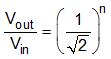
or, by tuning the cutoff point further away from the PWM frequency, achieved here by increasing C2 to 420 pF (see Figure 1-4). However, the criterion for the previous fC equation is violated; therefore the frequency (549Hz in this example) is now obtained by Equation 5.
Additionally, the DC level can be changed by adjusting the duty cycle of the DC PWM (see Figure 1-3 and Figure 1-4). These values are directly proportional (attenuation may need to be accounted for depending on filter design) and follow the relationship:
where, D = PWM duty cycle.
 Figure 1-4 250Hz RC Filtered Sine
Wave
Figure 1-4 250Hz RC Filtered Sine
WaveSimilarly, a ramp signal can be generated by commenting out the sine table code and uncommenting the ramp signal code in the ISR. Figure 1-5 depicts the output of the ramp function.
 Figure 1-5 Ramp Signal
When using the GUI enabled project, the TimerA clock source uses the 32 kHz ACLK to generate a 4Hz to 16Hz sine wave, a 0.5 to 2Hz ramp signal, or a DC signal that can be captured, communicated and visualized via a 9600 baud Universal Asynchronous Receiver/Transmitter (UART) to a PC GUI. The RC circuit used for both static and time variant outputs is modified for a cutoff frequency of 5Hz with a C value of 0.1 μF and an R value of 332KΩ.
 Figure 1-6 GUI Image
As can be seen from Figure 1-6, PWM0 is configured to output a sine wave while PWM1 is configured to output a ramp. The frequency of the sine wave will be 8x higher than the frequency of the ramp because the sine wave is generated via a table of 32 values while the ramp is generated by incrementing a counter over 256 values. Because the frequency of the ADC captures will be limited by the amount of data that can be transmitted over the UART, higher sampling rates can be achieved by enabling one graph at a time.
To Get Started
- Watch the PWM DAC using a Housekeeping MCU training video to learn how to use the GUI to setup the PWMs and see the ADC captured output.
- Order a MSP430FR2433 LaunchPad Development Kit to evaluate the PWM DAC example GUI and code.
- Download and test the PWM DAC example GUI to easily setup the PWMs and see the ADC captured output.
- Evaluate the PWM DAC example code using the MSP430FR2433 LaunchPad Development Kit .
| Part Number | Key Features |
|---|---|
| MSP430FR2433 | 16KB FRAM, 4KB SRAM, 10-bit ADC, UART/SPI/I2C, Timer |
| MSP430FR2422 | 8KB FRAM, 2KB SRAM, 10-bit ADC, UART/SPI/I2C, Timer |