SLAAE35 March 2022 MSP430FR2355 , TLV9002
1 Application Brief
Introduction
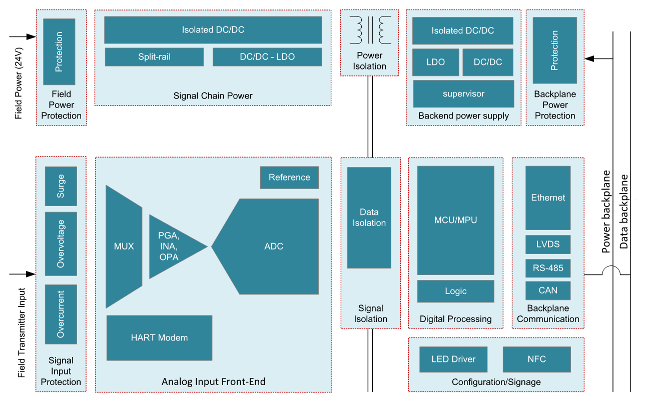
A Programmable Logic Controller (PLC) is a robust process control unit widely used in factory automation, such as manufacturing lines and automated robotic machinery. A similar centralized control unit, sharing many requirements and functionality with a PLC, is used in building automation applications, such as smart homes or building security systems.
An Analog Input Module (AIN) as a subsystem of a PLC, is the front end between the physical real world parameters (that is, Temperature, Distance, Humidity) and the fully digital control unit. The AIN can be implemented into the main PLC unit, but extendable modular systems and remote AINs are also widely used. The AIN command input and typical sensory output are single- or bipolar-voltage (that is, 0 V to 10 V) or current (that is, 0 mA to 20 mA) signals.
 Figure 1-1 AIN AFE EE Diagram
The accelerating industrial 4.0 revolution keeps increasing the demand for scalable and extendable AIN modules and the reduction of development time, board size, and costs. A possible implementation for a cost-optimized AIN architecture based on a MSP430FR2355 MCU with integrated analog functionality is introduced.
MSP430FR2355 With Integrated Analog
The MSP430FR2355 is a low-power, low-cost MCU with integrated analog features. It integrates a 12-bit SAR ADC and four configurable signal-chain modules called smart analog combos (SAC), each of which can be used as a 12-bit DAC or a configurable programmable-gain op amp to meet the specific needs of a system while reducing cost and PCB size.
| Channels | Up to 12 multiplexed channels |
| Resolution | 10- or 12-bit mode |
| Sample frequency | Up to about 200 kHz |
| Voltage reference | Internal 1.5-V, 2.0-V, and 2.5-V rails or external |
For a cost-sensitive entry or mid-performance AIN architecture an MCU-integrated ADC with low input voltage range in combination with an external front end is a good fit. Designing the input front-end with discrete components brings higher flexibility in meeting target requirements and reducing cost.
Voltage and Current Input Front End
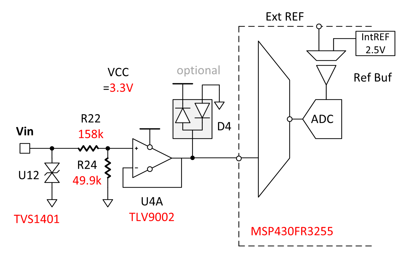
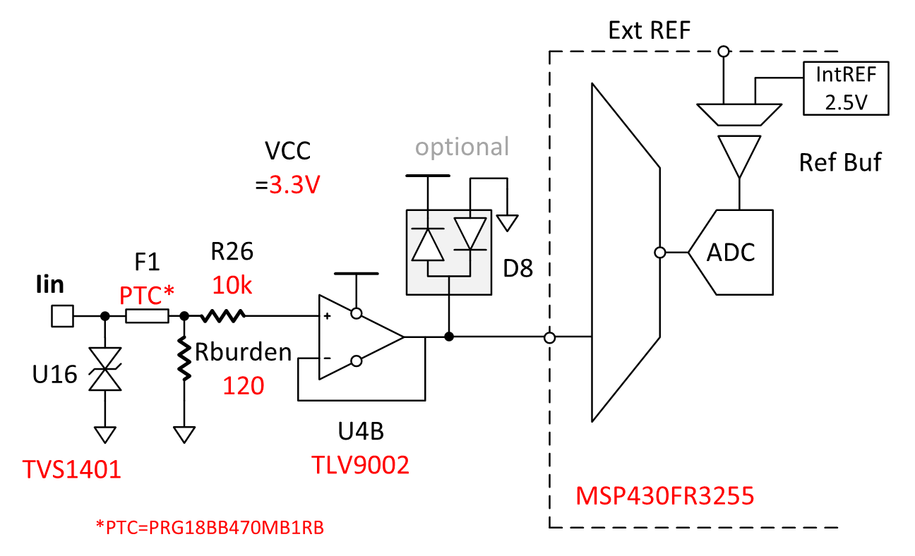
The Input Front End converts the industries typical signal input range (that is, 0 V to 10 V, 0 mA to 20 mA) to the ADCs input voltage range as well as setting the input impedance and providing required overvoltage and overcurrent protection. Figure 1-2 and Figure 1-3 show a discrete unipolar architecture targeting the ADC 2.5-V rail with focus on achieving system accuracy below 1% and optimizing cost.
 Figure 1-2 VIN Front End
| Requirement | Specification | |
|---|---|---|
| R1, R2 voltage divider | Trade off between accuracy and cost to achieve target system accuracy | 1%, 50ppm/°C |
| Op amp | TLV9002 | |
| Protection | Bidirectional surge protection, op-amp input protection | TVS1401, dual clamping diode |
 Figure 1-3 IIN Front End
| Requirement | Specification | |
|---|---|---|
| Shunt Resistor | Trade off between accuracy and cost to achieve target system accuracy | 1%, 50ppm/°C, 1 W |
| Op amp | TLV9002 | |
| Protection | Bidirectional surge protection, shunt protection, optional op-amp input protection | TVS1401, PTC, dual clamping diode |
The gain factor of the input stages is chosen so that the 10-V or 20-mA input signals result in an input voltage to the ADC a bit lower than the full-scale of 2.5 V to avoid saturation in consideration of offset, gain, and other errors. For the voltage input stage a gain of 0.24 V/V is used, that is, 2.4 V corresponds to the 10-V input. For the current input stage, a 20-mA input current over the 120-Ω shunt resistor results in 2.4 V at the ADC input.
System Accuracy
The achievable system accuracy is derived from the overall system error. Offset, gain, and other static errors can be eliminated implementing calibration with the cost of lowering the dynamic range. The MSP430FR2355 supports calibration registers for the ADC and the internal reference, for implementing a factory calibration.
There is flexibility to meet individual accuracy specification, choosing front end components (that is, specification of resistors, op amp, ext. reference).
Table 1-4 lists various error specifications, derived from the data sheets of the system components
| Resistors | Op Amp | int REF | REF Buffer | ADC | Unit | |
|---|---|---|---|---|---|---|
| 1%, 50ppm | TLV9002 | MSP430FR2355 | ||||
| Offset Error | 1.5 | 16 | 1.5 | mV | ||
| Offset Drift | 0.004 | mV/°C | ||||
| Gain Error | 1.25 (VIN) 1.00 (IIN) | 1.5 | 0.64 | 0.0732 | %FS | |
| Gain Drift | 50 | ppm/°C | ||||
| Noise | 130 | μV | ||||
These error values are referred to specific points in the signal chain. Consider the signal-chain gain when calculating the overall offset and gain errors at the input terminals. For example, a 1-mV offset at the input of the ADC corresponds to 1/2.4 mV = 4.167-mV offset at the input terminal.
Layout Size
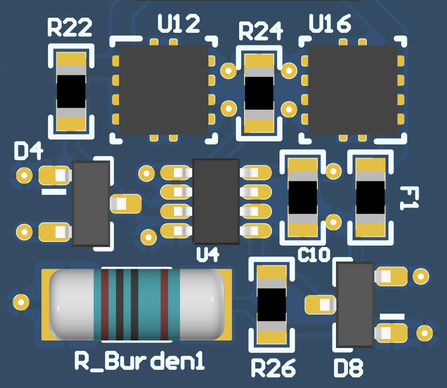
To demonstrate the size of the proposed circuit, both voltage and current input front-ends including the protection devices are placed on a single-sided PCB. Both channels require only 10 mm × 10 mm2 as shown in Figure 1-4. The effective front-end area per channel is approximately 5 × 10 mm2. Quad op-amp packages can be used instead of dual op amp and optional clamping diodes can be removed to further reduce the circuit area.
 Figure 1-4 VIN and IIN Layout
Measurement Procedure
For offset measurements the input is shorted to ground, while the FR2355 integrated ADC captures 1024 samples, from which the average value represents the offset values. If the offset is negative and cannot be measured directly from zero input, a slightly positive input of a few LSBs is added to determine the negative offset.
For measuring gain error the input signal is set to full-scale value. The ADC captures 1024 samples and the average value represents the full-scale error. The gain error is calculated by subtracting the offset error from the full-scale error.
To measure the signal-chain noise, DC voltage levels of 1.6 V, and 8.3 V are applied from battery cells, to minimize any added noise from the input source. The internal ADC captures 1024 samples, from which RMS noise is calculated. SNR and ENOBs are calculated with Equation 1 and Equation 2.
Measurement Results
Table 1-5 details the voltage input.
| Parameter | Conditions(1) | At 20°C | At –25°C | At 55°C | Unit |
|---|---|---|---|---|---|
| DC offset | 2.71 (6.89) | N/A(2) | 30.1 (76.5) | LSB (mV) | |
| Gain error | 7.27 (18.47) | 21.4 (–54.5) | LSB (mV) | ||
| FS error | 9.97 (25.37) | 23 (58.5) | 8.6 (22) | LSB (mV) | |
| RMS noise | 1.6-V DC input 8.3-V DC input | 1.03 (2.61) 1.68 (4.27) | 2.3 (5.8) | 0.76 (1.9) 1.9 (4.9) | LSB (mV) LSB (mV) |
| SNR | 1.6-V DC input 8.3-V DC input | 71.7 67.4 | 64.7 | 74.2 66.1 | |
| ENOB | 1.6-V DC input 8.3-V DC input | 11.6 10.9 | 10.5 | 12.0 10.7 | Bits |
Table 1-6 lists the current input parameter.
| Parameter | Conditions(1) | At 20°C | At –25°C | At 55°C | Unit |
|---|---|---|---|---|---|
| FS error | 3.26 (16.57) | 28.4 (144) | 18.3 (93) | LSB (μA) | |
| RMS noise | 19.652-mA DC input | 1.7 (8.5) | 2 (10.4) | 1.4 (7.2) | LSB (μA) LSB (μA) |
SNR | 19.652-mA DC input | 67.5 | 65.7 | 69.0 | |
| ENOB | 19.652-mA DC input | 10.9 | 10.6 | 11.1 | Bits |
The results for the current input stage are almost identical to these of the voltage input stage, with the burden resistors errors considered instead of the resistor divider.
The measurement results confirm the preliminary estimation of the offset error, gain error, and noise. The circuit maintains a minimum level of 10 b ENOBs over the temperature range, which can be further improved by running averaging over multiple samples. The offset and gain error can be reduced or eliminated by calibration. Single point calibration can be done in addition to correction based on the approximate temp measured by the MCU.
References
- Texas Instruments, MSP430FR4xx and MSP430FR2xx Family User's Guide
- Texas Instruments, MSP430FR235x, MSP430FR215x Mixed-Signal Microcontrollers Data Sheet
- Texas Instruments, Designing With the MSP430FR4xx and MSP430FR2xx ADC Application Report
- Texas Instruments, MSP430 ADC calibration – E2E™ Forum